Schematic | Circuit guide | Manual Wiring diagram | Electronic
Showing posts with label supply. Show all posts

Shift Register Driver Power Supply Circuit Diagram

Posted by Unknown Tuesday, December 24, 2013 0 comments
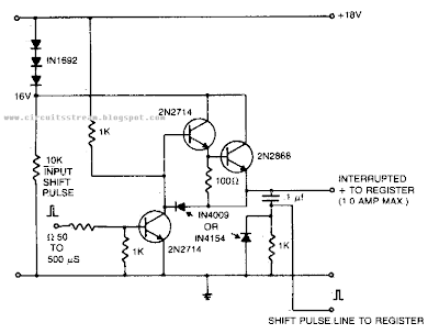
This is the Shift Register Driver Power Supply Circuit Diagram. A16 V power supply can be synthesized as shown using IN1692 rectifiers. A shift pulse input saturates the 2N2714 depriving the Darling-ton combination (2N2714 and 2N2868) of base drive.The negative pulse so generated on the 15 V line is differentiated to produce a positive trigger pulse at its trailing edge.

Shift Register Driver Power Supply Circuit Diagram

Shift Register Driver Power Supply Circuit Diagram

Build a Lcd Display Power Supply Circuit Diagram

Posted by Unknown Thursday, December 19, 2013 0 comments
This is the simple Lcd Display Power Supply Circuit Diagram. Laptop computers often use large-screen LCDs, which require a variable and a negative supply to ensure maximum contrast. This circuit operates from the system`s positive battery supply and generates a digitally variable negative voltage to drive the display. This figure`s switching regulator creates a negative voltage from the battery supply. The microprocessor data bus drives a 4-bit DAC, which in turn varies the actual regulator output from - 6.5 to -11.5 V. 

Lcd Display Power Supply Circuit Diagram


This arrangement allows a staircase of 16 possible voltages between these limits. The circuit implements the DAC by using the rail-to-rail output-drive capability of a 74 HC-series CMOS gate. A resistor divider network formed by the 240-kfi resistor, connected to the -V filter capacitor and the resistors, is referenced to the 5-V supply control (the MAX635 regulator). 

When the voltage at the VFb pin is greater than ground, the switching regulator turns on. The inductor dumps this energy into the -V filter capacitor. When the voltage at VFb is less than ground, the regulator skips a cycle. The MAX635 regulates the voltage at the junction of the resistor divider to 0 V. Thus, any resistor that the DAC connects to ground (logic 0) will not contribute any current to the ladder. Only the resistors that are at 5 V (logic 1) will be part of the voltage-divider equation. 

The entire switching-regulator supply draws less than 150 . You can place the circuit in an even lower power mode by interrupting the ground pin. The high-current path is from the battery input through the internal power PMOSFET to the external inductor. Disconnecting the ground connection simply disables the gate drive to the FET and turns off the internal oscillator.

3V Supply Splitter

Posted by Unknown Monday, October 7, 2013 0 comments
Many modern circuits tend to work from a single supply voltage of 3V. But often they need a virtual earth at half the supply voltage for efficient operation. The splitter shown in the diagram bisects the supply voltage with a high-resistance potential divider, R1-R2, and buffers the resulting 1.5 V line with an op amp. Since the op amp used is not a fast type, the output is decoupled by capacitive divider C2-C3. This ensures that the impedance of the virtual earth point remains low over a wide frequency band. Because the potential at the junction C2-C3-R3 is fed back to the inverting input of IC1, the circuit becomes a standard voltage follower.

Resistor R3 ensures that the regulation remains stable. The circuit can regulate ±2mA without any difficulties. Because of the low current drawn by IC1, and the high resistance of R1 and R2, the overall current drain is low. In the absence of a load, it was 13µA in the prototype, of which 1.5µA flows through R1-R2. Finally, since IC1 can operate from a voltage as low as 1.6V, the splitter will remain fully operational when the battery nears the end of its charge or life.

Dual Power Supply For Amplifiers

Posted by Unknown Sunday, September 22, 2013 0 comments
A power supply suitable for use with the 60W amplifier presented in the predeeding project is perfectly simple, and no great skill is required to build (or design) one. There are a few things one should be careful with, such as the routing of high current leads, but these are easily accomplished. The first thing to choose is a suitable transformer. I suggest toroidal transformers rather than the traditional "EI" laminated types because they radiate less magnetic flux and are flatter, allowing them to be installed in slimmer cases.

They do have some problems, such as higher inrush current at switch on, which means that slow blow fuses must be used. For the 60W amplifier, a nominal (full load) supply of +/- 35V is required, so a 25-0-25 secondary is ideal - however, see Updates, below. The circuit for the supply is shown below, and uses separate rectifiers, capacitors and fuses for each channel. Only the transformer is shared, so channel interactions are minimised. A single ±35V supply (i.e. using only a single bridge and set of filter capacitors) will work just as well in the majority of cases.

Dual Power Supply circuit diagram For AmplifiersThe 5A slow-blow fuse shown is suitable for a 300VA transformer, if a 120VA transformer is used, this should be reduced to 2.5A (or 3A if 2.5A proves too hard to get). If you are even a little bit concerned about the fuse rating, contact the transformer manufacturer for the recommended value for the transformer you will use. The correct fuse is critical to ensure safety from electrical failure, which could result in the equipment becoming unsafe or causing a fire.

The capacitance used is not critical, but is somewhat dependent upon ones budget. I suggest 10,000uF capacitors, but they are rather expensive so at a pinch 4,700uF caps should be fine - especially in the arrangement shown. When unloaded (or with only light load), the voltage will normally be somewhat higher than 35 Volts. This is Ok, and should not cause distress to any amp. The voltage will fall as more current is drawn, and may drop below 35V if a small transformer (or one with unusually poor regulation) is used.

Two parts of this circuit are critical:
  • Mains wiring must be cabled using approved 240V rated insulated cable, and all terminations must be insulated to prevent accidental contact. The mains earth must be securely fastened to the chassis, after scraping away any paint or other coating which might prevent reliable contact.
  • The centre-tap of the transformer and the ground points of each capacitor must be connected to the main signal earth point via heavy duty copper wire, or (preferably) a copper bus-bar. Large currents flow in this part of the circuit, containing nasty current waveforms which are quite happy to invade your amplifier. The supply voltages must be taken from the capacitors (not the bridge rectifiers) to prevent unwanted hum and noise.
When wiring the bridge rectifiers to the transformer, connect exactly as shown to ensure that ripple voltages (and currents) are in phase for each amp. If not, mysterious hum signals may be injected into the amps signal path from bypass capacitors and the like. This is somewhat unlikely unless huge caps are used on the amp board(s) - not recommended, by the way - but why take the risk?

Bridge rectifiers should be the big bolt-down 35A types (or something similar) to ensure lowest possible losses (these will not require an additional heatsink - the chassis will normally be quite sufficient). The transformer primary voltage will obviously be determined by the supply voltage in your area (i.e. 120, 220 or 240) and be suited to the local supply frequency. Note that all 50Hz transformers will work just fine at 60Hz, but some 60Hz devices will overheat if used at 50Hz.

The transformer should be rated at a minimum of 120VA (Volt-Amps) for home use, but a 300VA transformer is recommended due to its superior regulation. Going beyond 300VA will serve no useful purpose, other than to dim the lights as it is turned on. Where it is possible, the signal and power ground should be the same (this prevents the possibility of an electric shock hazard should the transformer develop a short circuit between primary and secondary. Where this will give rise to ground loops and hum in other equipment, use the method shown.

The resistor R1 (a 5W wirewound resistor is suggested) isolates the low-voltage high-current ground loop circuit, and the diodes D1 & D2 provide a protective circuit in the event of a major problem. These diodes need only be low voltage, but a current rating of 5A or greater is required. The 100nF capacitor (C1) acts as a short circuit to radio frequency signals, effectively grounding them. This should be a device with very good high frequency response, and a monolithic ceramic is recommended.

Updates:

The transformer secondary voltage will probably need to be higher than described above. I tested some stock and custom transformers I have, and found that unless the transformer has extraordinarly good regulation, a nominal 28-0-28 secondary will be needed, more with an average (i.e. poor) regulation unit. Also be careful when you test, since a relatively small (10%) variation in the mains voltage makes a big difference to measured output power - the secondary voltage also falls by 10%, so 60W becomes 48W if the mains is 10% low.

You also need to remember that the output voltage of transformers is typically quoted at full power with a resistive load. This means two things:
  1. The no load voltage will be higher than expected
  2. The loaded voltage will be lower than expected
The first point is true because there is no loading, so the output voltage must rise. The second is more complex, but happens because the conventional rectifier circuit uses a capacitor input filter (the rectifier feeds directly into the capacitor(s)). Since the diodes only conduct at the peak of the waveform, the current is much higher, so the transformer and supply line impedance will cause the peak voltage to fall, and the DC voltage cannot exceed the peak output voltage (less two diode forward voltage drops).
Source: http://sound.westhost.com/project04.htm
Antique Radio Dc Filament Supply Circuit Diagram

Posted by Unknown Wednesday, August 14, 2013 0 comments
This dc supply is great for operating battery-powered antique radios, because it is designed to prevent harming the tube filaments. The circuit is useful for powering filaments of 00-A, 01-A, 112A, and 71A tubes, which require 5V at 250 mA. 


 Antique Radio Dc Filament Supply Circuit Diagram


6 12 Volt Adjustable Power Supply Circuit

Posted by Unknown Tuesday, August 13, 2013 0 comments
adsjust power supply
Power Supply in this article use a regulator that is composed of 2 pieces of NPN transistor. A transistor acts as a power regulator and a transistor again serves as a controller output voltage.


Power Supply has an adjustable output with a range of 6-12 VDC. The part that serves as a power regulator is Q1 TIP31. Then the controller output voltage is a voltage divider composed of R3, R4, VR1 and R2 provide bias to the base of Q2 to Q1 mengentrol power regulator. In a series of power supply is mounted 5.1 V zener diode which serves to make the minimum limit the output voltage with Q2.
6 - 12 Volt | Adjustable Power Supply Circuit
Adjustable Power Supply with transistor circuit

Power Supply With transistor circuit is quite simple and can be made with the PCB holes, so for those who want to try to directly mempraktikannya. May the power supply circuit can be useful for readers, especially for friends who need a power supply circuit with the regulator transistor.

Power Supply Variable 1 3V 12 2V 1A Circuit

Posted by Unknown Monday, August 12, 2013 0 comments
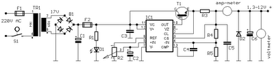
Power supply circuit to generate output below were variations between 1.3V DC to 12.2V DC with 1A current. In addition, the power supply circuit is also equipped with over-current protection or shield against belebih flow. Power supply circuit is very simple, but the quality is quite good, made her basiskan regulator IC LM723 is a pretty legendary.


1.3V DC to 12.2V DC Regulator Power Supply


Description:

R2 to set the output voltage. The maximum current is determined by R3, over-current protection circuit inside the LM723 to detect the voltage on R3, if it reaches 0.65 V, the voltage output will be off her. So the current through R3 can not exceed 0.65 / R3 although output short-circuit in his.


C3 and C4 are ceramic capacitors, as much as possible directly soldered to the PCB, this is because the LM723 is prone to oscillation that is not cool.


LM723 works with 9.5V input voltage to 40 V DC and the LM723 can generate its own current of 150mA when the output voltage is not more than 6-7V under input voltage.


Specifications:

Output (value estimated):


Vmin = (R4 + R5) / (R5 * 1.3)

Vmax = (7.15 / R5) * (R4 + R5)


Imax = 0.65/R3


Max. Power on R3: 0.42/R3


Min. DC Input Voltage (pin 12 to pin 7): Vmax + 5


Component List:

B1 40V/2.5A

C1 2200uF (3300uF even better)

C2 4.7uF

C3 100nF

C4 1NF

C5 330nF

C6 100uF

Green LED D1

D2 1N4003

F1 0.2A F

F2 2A M

IC1 LM723 (in a DIL14 plastic package)

R1 1k

R2 Pot. 5k

R3 0.56R/2W


R4 3.3k

R5 4.7k

S1 250V/1A

T1 2N3055 on a heatsink 5K / W

TR1 220V/17V/1.5

Supply Voltage Monitor

Posted by Unknown Saturday, August 10, 2013 0 comments
A circuit for monitoring supply voltages of ±5 V and ±12 V is readily constructed as shown in the diagram. It is appreciably simpler than the usual monitors that use comparators, and AND gates. The circuit is not intended to indicate the level of the inputs. In normal operation, transistors T1 and T3 must be seen as current sources. The drop across resistors R1 and R2 is 6.3 V (12 –5 –0.7). This means that the current is 6.3mA and this flows through diode D1 when all four voltages are present. However, if for instance, the –5 V line fails, transistor T3 remains on but the base-emitter junction of T2 is no longer biased, so that this transistor is cut off. When this happens, there is no current through D which then goes out.

supply voltage monitorw Circuit diagram


Streampowers

Build a high volt supply Circuit Diagram

Posted by Unknown Sunday, August 4, 2013 0 comments
A light dimmer, a 1 µf capacitor and a 12 V car ignition coil form the simple line powered HV generator. The current in the dimmer is shown in Fig. B. At times tp t2, set by the dimmer switch, the inner triac of the dimmer switches on, and a very high and very fast current pulse charges the capacitor through the primary of the induction coil. 

Then at a rate of 120 times per second for a 60 Hz line, a very high voltage pulse appears at the secondary of the coil. To obtain an HV dc output, use a voltage doubler. Dl and D2 are selenium rectifiers (TV 18 Siemens or ITT) used for the supply of television sets. High value output shock protection resistors, R, are recommended when suitable. 

 Build a high-volt supply Circuit Diagram

Build a high-volt supply Circuit Diagram

12V DC Switch Mode Power Supply Rise

Posted by Unknown Friday, August 2, 2013 0 comments
Basic Of Switch Mode Power Supply
In recent years, the use of switch mode power supply (SMPS) has become more comon as more applications demand for greater power eficiency. It makes use of semiconductor (mostly MOSFET) fast switches to switch DC input that has been rectified at high frequency. The advantages of high frequency switching are that it reduces the size of inductor, capacitors & transformer used. Other advantages of switching power supply over linear power supply are :

1) High Efficiency (up to 90% and above for nice design).
2) Output can be higher than input.
3) Able to operate over a variety of input power supply.
4) Able to have over output.

The setback of using SMPS compared to linear power supply is that it generates electrical noise which contributes to electromagnetic compatibility design issues & more part count.

Buck Converter SMPS
The SMPS circuit below from Power Integration makes use of LNK304 as its high frequency switch. Take note that this circuit is non isolated type which means that the output is not electrically isolated from the input & all testing ought to be completed using an isolation transformer to provide the AC line input to the board.

Make positive that you have electrical safety knowledge & experience before you embark on doing this project.

The features of this project is as summarized below.

Input : 85-265 VAC
Output : 12 V, 120 mA, 1.44 Watt
Low Cost : Only 16 components are needed
No-load power consumption : < 0.2 Watt


Very Low Dropout Adjustable Breadboard Power Supply

Posted by Unknown Wednesday, July 31, 2013 0 comments
This project details the design of a very low dropout adjustable power supply. A good power supply is essential to electronic projects. While there are many existing designs for adjustable power supplies, this one makes improvements that make it more useful for hobby designs

Very Low Dropout Adjustable Breadboard Power SupplyMIC2941 regulator has guaranteed 1.25A output
Low dropout, only 40mV - 400mV compared to 1.25V - 2.0V for LM317. This means you can use a wider range of output voltages including generating 3.3V from as low as 3.7V (such as 3 AAs or a lithium ion battery)!
Short circuit and overheating protection
Input diode to protect circuitry from negative voltages or AC power supplies.
2.1mm DC jack and terminal connector for voltage inputs
Two indicator LEDs for high and low voltages
Output selection switch to select from 3.3v, 5v and Adjustable
On-board potentiometer for adjusting voltage from 1.25V up to within 0.5V of the input voltage. (20V max)
On/Off switch for entire board
Very Low Dropout Adjustable Breadboard Power Supply Circuit Diagram

13 8Vdc 2A Regulated Power Supply Circuit Diagram

Posted by Unknown Thursday, July 25, 2013 0 comments
This 13.8Vdc 2A Regulated Power Supply Circuit Diagram consists of step-down transformer Tl, a full-wave rectifier bridge (D1 through D4), and a filtering regulator circuit made up of Cl, C2, Rl, R2, R8, D5, and Ql, When 120 Vac is provided, the neon-lamp assembly LI lights up, and transformer Tl changes 120 Vac to about 28 Vac. 

The rectifier bridge, )1 through D4, rectifies the ac into pulsating dc, which is then filtered by Cl. Capacitor Cl acts as a storage capacitor. Zener diode 1)5 keeps the voltage constant across the base of Darlington regulator Ql, causing constant voltage across resistor R3 and the (+) and (-) output terminals, where the load is connected. Fuse F2 is used to open (blow), if the current through the output terminals is too high. Make sure to take proper precautions when using projects powered by 120 Vac.

 13.8Vdc 2A Regulated Power Supply Circuit Diagram


13.8Vdc 2A Regulated Power Supply Circuit Diagram

Adjustable 1 3 22V Regulated Power Supply

Posted by Unknown Wednesday, May 29, 2013 0 comments
Want a regulated voltage that can be adjusted to suit your application? This Adjustable Power Supply is small, easy to build and can be adapted to produce a fully regulated voltage ranging from 1.3V to 22V at currents up to 1A. This circuit come from SiliconChip Magazine

There are many fixed-voltage IC regulators available and these can be had with 5V, 6V 8V, 9V, 12V & 15V outputs. But what if you want a voltage output that does not fit into one of the standard ranges or if you want to be able to easily adjust this output voltage? An adjustable regulator is the answer – one that can be set to provide the exact voltage you require.

This Adjustable Power Supply comprises a small PC board that utilises a 3-terminal regulator. It does not have too many other components – in fact, there are just three diodes, three capacitors, a resistor and a trimpot to set the output voltage from the regulator. The circuit is based on an LM317T adjustable voltage regulator. D1 provides reverse polarity protection while P1 sets the output voltage.

Project looks like:
picture of the project
Picture Of The Project
Parts layout:
Parts layout of regulated power supply
Parts Layout Of The Project
PCB layout:
PCB layout for regulated power supply
PCB Layout Of The Project
Circuit diagram:
Adjustable 1.3-22V Regulated Power Supply
Adjustable Regulated DC Power Supply Circuit Diagram
Parts list:

IC = LM317T adjustable 3-terminal regulator
P1 = 2k horizontal trimpot
R1 = 110R-0.25W
C1 = 100uF-25V
C2 = 10uF-25V
C3 = 100uF-25V
D1 = 1N4004
D2 = 1N4004
D3 = 1N4004

LTC3588 1 Piezoelectric Energy Harvesting Power Supply Circuit

Posted by Unknown Monday, April 8, 2013 0 comments
Here’s a design circuit of The LTC3588-1 is a piezoelectric energy harvesting power supply IC that integrates a low-loss full-wave bridge rectifier with a high efficiency buck converter to form a complete energy harvesting solution optimized for high output impedance energy sources such as piezoelectric transducers. This is the figure of the circuit;


LTC3588-1 can be configured to deliver four output voltages: 1.8V, 2.5V, 3.3V and 3.6V. In this table you can see how you need to configure the pins of the LTC3588-1 to obtain the specified voltage.  To select Low for D0, D1 the pin must be connected to GND and if you need to select high for D0, D2 the pin must be connected to VIN2. The maximum output current can be set up to 100mA. As you can see in this power schematic circuit the design of power supply is very easy and require few external components. A power supply circuit based on the LTC3588-1 IC offers many features like: 950nA Input Quiescent Current (Output in Regulation – No Load) , 450nA Input Quiescent Current in UVLO, 2.7V to 20V Input Operating Range, Integrated Low-Loss Full-Wave Bridge Rectifier, Up to 100mA of Output Current, Selectable Output Voltages, High Efficiency Integrated Hysteretic Buck DC/DC.

The LTC3588-1 IC can be used in many applications circuits like: Piezoelectric Energy Harvesting, Electro-Mechanical Energy Harvesting, Wireless HVAC Sensors, Mobile Asset Tracking, Tire Pressure Sensors, Battery Replacement for Industrial Sensors, Remote Light Switches.

Power Supply Variable 1 3V 12 2V 1A Circuit

Posted by Unknown 0 comments
Power supply circuit to generate output below were variations between 1.3V DC to 12.2V DC with 1A current.
In addition, the power supply circuit is also equipped with over-current protection or shield against belebih flow. Power supply circuit is very simple, but the quality is quite good, made her basiskan regulator IC LM723 is a pretty legendary.


1.3V DC to 12.2V DC Regulator Power Supply


Description:

R2 to set the output voltage. The maximum current is determined by R3, over-current protection circuit inside the LM723 to detect the voltage on R3, if it reaches 0.65 V, the voltage output will be off her. So the current through R3 can not exceed 0.65 / R3 although output short-circuit in his.


C3 and C4 are ceramic capacitors, as much as possible directly soldered to the PCB, this is because the LM723 is prone to oscillation that is not cool.


LM723 works with 9.5V input voltage to 40 V DC and the LM723 can generate its own current of 150mA when the output voltage is not more than 6-7V under input voltage.


Specifications:

Output (value estimated):


Vmin = (R4 + R5) / (R5 * 1.3)

Vmax = (7.15 / R5) * (R4 + R5)


Imax = 0.65/R3


Max. Power on R3: 0.42/R3


Min. DC Input Voltage (pin 12 to pin 7): Vmax + 5


Component List:

B1 40V/2.5A

C1 2200uF (3300uF even better)

C2 4.7uF

C3 100nF

C4 1NF

C5 330nF

C6 100uF

Green LED D1

D2 1N4003

F1 0.2A F

F2 2A M

IC1 LM723 (in a DIL14 plastic package)

R1 1k

R2 Pot. 5k

R3 0.56R/2W


R4 3.3k

R5 4.7k

S1 250V/1A

T1 2N3055 on a heatsink 5K / W

TR1 220V/17V/1.5