Schematic | Circuit guide | Manual Wiring diagram | Electronic
Showing posts with label power. Show all posts

Shift Register Driver Power Supply Circuit Diagram

Posted by Unknown Tuesday, December 24, 2013 0 comments
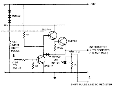
This is the Shift Register Driver Power Supply Circuit Diagram. A16 V power supply can be synthesized as shown using IN1692 rectifiers. A shift pulse input saturates the 2N2714 depriving the Darling-ton combination (2N2714 and 2N2868) of base drive.The negative pulse so generated on the 15 V line is differentiated to produce a positive trigger pulse at its trailing edge.

Shift Register Driver Power Supply Circuit Diagram

Shift Register Driver Power Supply Circuit Diagram

Simple Power Pulse Using by LM350 and NE555 Circuit Diagram

Posted by Unknown Friday, December 20, 2013 0 comments
This is a Simple Power Pulse Using by LM350 and NE555 Circuit Diagram. This circuit can use to drive lamp,power LED,DC motor etc. Adjust R5 for output amplitude.Adjust R1 for output power .

Power Pulse Circuit Diagram

Power Pulse Circuit Diagram


The LM350 is adjustable 3-terminal positive voltage regulators is capable of supplying in excess of 3A over a 1.2V to 33V output range.This circuit requires 5-15V power supply.

Build a Lcd Display Power Supply Circuit Diagram

Posted by Unknown Thursday, December 19, 2013 0 comments
This is the simple Lcd Display Power Supply Circuit Diagram. Laptop computers often use large-screen LCDs, which require a variable and a negative supply to ensure maximum contrast. This circuit operates from the system`s positive battery supply and generates a digitally variable negative voltage to drive the display. This figure`s switching regulator creates a negative voltage from the battery supply. The microprocessor data bus drives a 4-bit DAC, which in turn varies the actual regulator output from - 6.5 to -11.5 V. 

Lcd Display Power Supply Circuit Diagram


This arrangement allows a staircase of 16 possible voltages between these limits. The circuit implements the DAC by using the rail-to-rail output-drive capability of a 74 HC-series CMOS gate. A resistor divider network formed by the 240-kfi resistor, connected to the -V filter capacitor and the resistors, is referenced to the 5-V supply control (the MAX635 regulator). 

When the voltage at the VFb pin is greater than ground, the switching regulator turns on. The inductor dumps this energy into the -V filter capacitor. When the voltage at VFb is less than ground, the regulator skips a cycle. The MAX635 regulates the voltage at the junction of the resistor divider to 0 V. Thus, any resistor that the DAC connects to ground (logic 0) will not contribute any current to the ladder. Only the resistors that are at 5 V (logic 1) will be part of the voltage-divider equation. 

The entire switching-regulator supply draws less than 150 . You can place the circuit in an even lower power mode by interrupting the ground pin. The high-current path is from the battery input through the internal power PMOSFET to the external inductor. Disconnecting the ground connection simply disables the gate drive to the FET and turns off the internal oscillator.

11W Stereo 22W Mono Power Amp Using TDA1519C

Posted by Unknown Tuesday, September 24, 2013 0 comments
Integrated AF power amps have seen great improvements in recent years offering improved power and easier use. The TDA1519C from Philips contains two power amplifiers providing 11 W per channel stereo or 22 W mono when the two channels are connected in a bridge configuration. The special in-line SIL9P package outline allows the chip to be conveniently bolted to a suitable heatsink. The TDA1519CSP is the SMD version, in this case the heat sink is mounted over, and in contact with, the top surface of the chip.

11W Stereo Mono Power Amp Circuit Diagram Using TDA1519C
The operating voltage of this device is from +6V to +17.5V. The two channels of the amplifier are different in that one channel, between pins 1 and 4, is a non-inverting amplifier, while the other between pins 9 and 6 is an inverting amplifier. It is therefore necessary in stereo operation, to wire the speakers so that one of them has its polarity reversed. Each amplifier has an input impedance of 60kΩ and a voltage gain of 40dB, i.e. 100 times. When both amplifier are used in a bridge configuration, the inputs are in parallel so that the input impedance will be 30kΩ.

22W Mono Power Amp Circuit Diagram Using TDA1519C
A combined mute/standby function is provided on pin 8. In its simplest form this can be connected to the positive rail via a switch. When the switch is open the amplifier will be in standby mode and current consumption is less than 100µA. When the switch is closed, the amplifier will be operational. A circuit is also shown that uses the mute input to prevent the annoying switch-on plop heard when power amps are first switched on This is caused by the rush of current to charge capacitors C1 and C2.

standby switch circuit diagram
The circuit shown generates a ramp voltage, which is applied to pin 8. At switch on, as the voltage rises from 3.3 V to 6.4 V, the amplifier will switch out of standby mode and into mute mode allowing C1 and C2 to charge. Only when the ramp voltage on pin 8 reaches 8.5V will the amplifier switch into active mode. Protection built into the TDA1519C would seem to make it almost foolproof. The two outputs can be shorted to either of the supply rails and to each other. A thermal shutdown will prevent overloading and the power supply input is protected against accidental reversal of the supply leads up to 6V.

Dual Power Supply For Amplifiers

Posted by Unknown Sunday, September 22, 2013 0 comments
A power supply suitable for use with the 60W amplifier presented in the predeeding project is perfectly simple, and no great skill is required to build (or design) one. There are a few things one should be careful with, such as the routing of high current leads, but these are easily accomplished. The first thing to choose is a suitable transformer. I suggest toroidal transformers rather than the traditional "EI" laminated types because they radiate less magnetic flux and are flatter, allowing them to be installed in slimmer cases.

They do have some problems, such as higher inrush current at switch on, which means that slow blow fuses must be used. For the 60W amplifier, a nominal (full load) supply of +/- 35V is required, so a 25-0-25 secondary is ideal - however, see Updates, below. The circuit for the supply is shown below, and uses separate rectifiers, capacitors and fuses for each channel. Only the transformer is shared, so channel interactions are minimised. A single ±35V supply (i.e. using only a single bridge and set of filter capacitors) will work just as well in the majority of cases.

Dual Power Supply circuit diagram For AmplifiersThe 5A slow-blow fuse shown is suitable for a 300VA transformer, if a 120VA transformer is used, this should be reduced to 2.5A (or 3A if 2.5A proves too hard to get). If you are even a little bit concerned about the fuse rating, contact the transformer manufacturer for the recommended value for the transformer you will use. The correct fuse is critical to ensure safety from electrical failure, which could result in the equipment becoming unsafe or causing a fire.

The capacitance used is not critical, but is somewhat dependent upon ones budget. I suggest 10,000uF capacitors, but they are rather expensive so at a pinch 4,700uF caps should be fine - especially in the arrangement shown. When unloaded (or with only light load), the voltage will normally be somewhat higher than 35 Volts. This is Ok, and should not cause distress to any amp. The voltage will fall as more current is drawn, and may drop below 35V if a small transformer (or one with unusually poor regulation) is used.

Two parts of this circuit are critical:
  • Mains wiring must be cabled using approved 240V rated insulated cable, and all terminations must be insulated to prevent accidental contact. The mains earth must be securely fastened to the chassis, after scraping away any paint or other coating which might prevent reliable contact.
  • The centre-tap of the transformer and the ground points of each capacitor must be connected to the main signal earth point via heavy duty copper wire, or (preferably) a copper bus-bar. Large currents flow in this part of the circuit, containing nasty current waveforms which are quite happy to invade your amplifier. The supply voltages must be taken from the capacitors (not the bridge rectifiers) to prevent unwanted hum and noise.
When wiring the bridge rectifiers to the transformer, connect exactly as shown to ensure that ripple voltages (and currents) are in phase for each amp. If not, mysterious hum signals may be injected into the amps signal path from bypass capacitors and the like. This is somewhat unlikely unless huge caps are used on the amp board(s) - not recommended, by the way - but why take the risk?

Bridge rectifiers should be the big bolt-down 35A types (or something similar) to ensure lowest possible losses (these will not require an additional heatsink - the chassis will normally be quite sufficient). The transformer primary voltage will obviously be determined by the supply voltage in your area (i.e. 120, 220 or 240) and be suited to the local supply frequency. Note that all 50Hz transformers will work just fine at 60Hz, but some 60Hz devices will overheat if used at 50Hz.

The transformer should be rated at a minimum of 120VA (Volt-Amps) for home use, but a 300VA transformer is recommended due to its superior regulation. Going beyond 300VA will serve no useful purpose, other than to dim the lights as it is turned on. Where it is possible, the signal and power ground should be the same (this prevents the possibility of an electric shock hazard should the transformer develop a short circuit between primary and secondary. Where this will give rise to ground loops and hum in other equipment, use the method shown.

The resistor R1 (a 5W wirewound resistor is suggested) isolates the low-voltage high-current ground loop circuit, and the diodes D1 & D2 provide a protective circuit in the event of a major problem. These diodes need only be low voltage, but a current rating of 5A or greater is required. The 100nF capacitor (C1) acts as a short circuit to radio frequency signals, effectively grounding them. This should be a device with very good high frequency response, and a monolithic ceramic is recommended.

Updates:

The transformer secondary voltage will probably need to be higher than described above. I tested some stock and custom transformers I have, and found that unless the transformer has extraordinarly good regulation, a nominal 28-0-28 secondary will be needed, more with an average (i.e. poor) regulation unit. Also be careful when you test, since a relatively small (10%) variation in the mains voltage makes a big difference to measured output power - the secondary voltage also falls by 10%, so 60W becomes 48W if the mains is 10% low.

You also need to remember that the output voltage of transformers is typically quoted at full power with a resistive load. This means two things:
  1. The no load voltage will be higher than expected
  2. The loaded voltage will be lower than expected
The first point is true because there is no loading, so the output voltage must rise. The second is more complex, but happens because the conventional rectifier circuit uses a capacitor input filter (the rectifier feeds directly into the capacitor(s)). Since the diodes only conduct at the peak of the waveform, the current is much higher, so the transformer and supply line impedance will cause the peak voltage to fall, and the DC voltage cannot exceed the peak output voltage (less two diode forward voltage drops).
Source: http://sound.westhost.com/project04.htm
100 W Bipolar Power Amplifier

Posted by Unknown Tuesday, September 3, 2013 0 comments
This is a basic 100 watt power amplifier designed to be (relatively) easy to build at a reasonable price. It has a better performance (read: musical quality) than the standard STK module amps that are used in almost every mass market stereo receiver manufactured today.

100 W Bipolar Power Amplifier Circuit Diagram


When I originally built this thing, it was because I needed a 100 WPC amp and do not want any money. So I designed around parts I had in the store. The design is actually a standard format, and I’m sure there are commercial entities that are similar. To my knowlwdge, it is not an exact copy of a commercial entity, nor am I aware of any patents on topology.

For experienced builders: I am aware that many improvements and adjustments can be made, but the idea was to keep it simple and must do-able by anyone who is a circuit, and has not the patience to do a sloppy job. If friend want Bipolar Transistor power amplifier circuit. , In model HIFI OCL 100W RMS. I think this track should be an interesting choice, this circuit is the use of the key transistor BD317 and BD318 unless transistor number BD139, BD140, BC556 too easy then try to buy when the 35V power source with only then build is not difficult for other details as the result of a few See Circuit.

Input stage is a BC556 transistor, which most of the open loop gain, and on the serene DC voltage stabilizes. This feeds a level shift stage where the voltage swing to (-) track references. The Transconductance stage is a Darlington, improve frerqency high linearity. The BD317, 318 on a rather large collector-base capacity is dependent on voltage. The BD319 presents this low-z and has a C (ob) of only a few of PF, which is effectively swamped by the pole-splitting 220pF cap. The scene is supplied by BC546 active load (current), which is approximately 20 mA. The current, until the BC556 is limited to about 70 mA in the worst cases.

6 12 Volt Adjustable Power Supply Circuit

Posted by Unknown Tuesday, August 13, 2013 0 comments
adsjust power supply
Power Supply in this article use a regulator that is composed of 2 pieces of NPN transistor. A transistor acts as a power regulator and a transistor again serves as a controller output voltage.


Power Supply has an adjustable output with a range of 6-12 VDC. The part that serves as a power regulator is Q1 TIP31. Then the controller output voltage is a voltage divider composed of R3, R4, VR1 and R2 provide bias to the base of Q2 to Q1 mengentrol power regulator. In a series of power supply is mounted 5.1 V zener diode which serves to make the minimum limit the output voltage with Q2.
6 - 12 Volt | Adjustable Power Supply Circuit
Adjustable Power Supply with transistor circuit

Power Supply With transistor circuit is quite simple and can be made with the PCB holes, so for those who want to try to directly mempraktikannya. May the power supply circuit can be useful for readers, especially for friends who need a power supply circuit with the regulator transistor.

Power Supply Variable 1 3V 12 2V 1A Circuit

Posted by Unknown Monday, August 12, 2013 0 comments
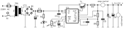
Power supply circuit to generate output below were variations between 1.3V DC to 12.2V DC with 1A current. In addition, the power supply circuit is also equipped with over-current protection or shield against belebih flow. Power supply circuit is very simple, but the quality is quite good, made her basiskan regulator IC LM723 is a pretty legendary.


1.3V DC to 12.2V DC Regulator Power Supply


Description:

R2 to set the output voltage. The maximum current is determined by R3, over-current protection circuit inside the LM723 to detect the voltage on R3, if it reaches 0.65 V, the voltage output will be off her. So the current through R3 can not exceed 0.65 / R3 although output short-circuit in his.


C3 and C4 are ceramic capacitors, as much as possible directly soldered to the PCB, this is because the LM723 is prone to oscillation that is not cool.


LM723 works with 9.5V input voltage to 40 V DC and the LM723 can generate its own current of 150mA when the output voltage is not more than 6-7V under input voltage.


Specifications:

Output (value estimated):


Vmin = (R4 + R5) / (R5 * 1.3)

Vmax = (7.15 / R5) * (R4 + R5)


Imax = 0.65/R3


Max. Power on R3: 0.42/R3


Min. DC Input Voltage (pin 12 to pin 7): Vmax + 5


Component List:

B1 40V/2.5A

C1 2200uF (3300uF even better)

C2 4.7uF

C3 100nF

C4 1NF

C5 330nF

C6 100uF

Green LED D1

D2 1N4003

F1 0.2A F

F2 2A M

IC1 LM723 (in a DIL14 plastic package)

R1 1k

R2 Pot. 5k

R3 0.56R/2W


R4 3.3k

R5 4.7k

S1 250V/1A

T1 2N3055 on a heatsink 5K / W

TR1 220V/17V/1.5

Linear RF Power Meter Circuit

Posted by Unknown Thursday, August 8, 2013 0 comments
The National Semiconductor LMV225 is a linear RF power meter IC in an SMD package. It can be used over the frequency range of 450 MHz to 2000 MHz and requires only four external components. The input coupling capacitor isolates the DC voltage of the IC from the input signal. The 10-k? resistor enables or disables the IC according to the DC voltage present at the input pin. If it is higher than 1.8 V, the detector is enabled and draws a current of around 5–8 mA. If the voltage on pin A1 is less than 0.8 V, the IC enters the shutdown mode and draws a current of only a few microampères. The LMV225 can be switched between the active and shutdown states using a logic-level signal if the signal is connected to the signal via the 10-kR resistor.
 
Circuit diagram:
linear-rf-power-meter-circuit-diagram1 Linear RF Power Meter Circuit Diagram
 
The supply voltage, which can lie between +2.7 V und +5.5 V, is filtered by a 100nF capacitor that diverts residual RF signals to ground. Finally, there is an output capacitor that forms a low-pass filter in combination with the internal circuitry of the LMV225. If this capacitor has a value of 1 nF, the corner frequency of this low-pass filter is approximately 8 kHz. The corner frequency can be calculated using the formula fc = 1 ÷ (2 p COUT Ro) where Ro is the internal output impedance (19.8 k?). The output low-pass filter determines which AM modulation components are passed by the detector.

rf-power-meter-circuit-diagram2
The output, which has a relatively high impedance, provides an output voltage that is proportional to the signal power, with a slope of 40 mV/dB. The output is 2.0 V at 9 dBm and 0.4 V at –40 dBm. A level of 0 dBm corresponds to a power of 1 mW in 50 R. For a sinusoidal wave-form, this is equivalent to an effective voltage of 224 mV. For modulated signals, the relationship between power and voltage is generally different. The table shows several examples of power levels and voltages for sinusoidal signals. The input impedance of the LMV225 detector is around 50 R to provide a good match to the characteristic impedance commonly used in RF circuits.

The data sheet for the LMV225 shows how the 40-dB measurement range can be shifted to a higher power level using a series input resistor. The LMV225 was originally designed for use in mobile telephones, so it comes in a tiny SMD package with dimensions of only around 1 × 1 mm with four solder bumps (similar to a ball-grid array package). The connections are labelled A1, A2, B1 and B1, like the elements of a matrix. The corner next to A1 is bevelled.

Streampowers

Reducing Relay Power Consumption

Posted by Unknown Saturday, August 3, 2013 0 comments
Relays are often used as electrically controlled switches. Unlike transistors, their switch contacts are electrically isolated from the control input. On the other hand, the power dissipation in a relay coil may be unattractive for battery-operated applications. Adding an analogue switch lowers the dissipation, allowing the relay to operate at a lower voltage. The circuit diagram shows the principle. Power consumed by the relay coil equals V2/RCOIL. The circuit lowers this dissipation (after actuation) by applying less than the normal operating voltage of 5 V. Note that the voltage required to turn a relay on (pickup voltage)is usually greater than that to keep it on (dropout voltage).


In this respect the relay shown has specifications of 3.5 and 1.5V respectively, yet the circuit allows it to operate from an intermediate supply voltage of 2.5V. Table 1 compares the relay’s power dissipation with fixed operating voltages across it, and with the circuit shown here in place. The power savings are significant. When SW1 is closed, current flows through the relay coil, and C1 and C2 begin to charge. The relay remains inactive because the supply voltage is less than its pickup voltage. The RC time constants are such that C1 charges almost completely before the voltage across C2 reaches the logic threshold of the analogue switch inside the MAX4624 IC.


When C2 reaches that threshold, the on-chip switch connects C1 in series with the 2.5V supply and the relay coil. This action causes the relay to be turned on because its coil voltage is then raised to 5 V, i.e., twice the supply voltage. As C1 discharges through the coil, the coil voltage drops back to 2.5 V minus the drop across D1. However, the relay remains on because the resultant voltage is still above the dropout level (1.5 V). Component values for this circuit depend on the relay characteristics and the supply voltage. The value of R1, which protects the analogue switch from the initial current surge through C1, should be sufficiently small to allow C1 to charge rapidly, but large enough to prevent the surge current from exceeding the specified peak current for the analogue switch.

The switch’s peak current (U1) is 400mA, and the peak surge current is IPEAK = (VIN – VD1) / R1 + RON) where RON is the on-resistance of the analogue switch (typically 1.2 Ω). The value of C1 will depend on the relay characteristics and on the difference between VIN and the pickup voltage. Relays that need more turn-on time requires larger values for C1. The values for R2 and C2 are selected to allow C1 to charge almost completely before C2’s voltage reaches the logic threshold of the analogue switch. In this case, the time constant R2C2 is about seven times C1(R1 + RON). Larger time constants increase the delay between switch closure and relay activation. The switches in the MAX4624 are described as ‘guaranteed break before make’. The opposite function, ‘make-before break’ is available from the MAX4625. The full datasheets of these interesting ICs may be found at http://pdfserv.maxim-ic.com/arpdf/MAX4624-MAX4625.pdf

12V DC Switch Mode Power Supply Rise

Posted by Unknown Friday, August 2, 2013 0 comments
Basic Of Switch Mode Power Supply
In recent years, the use of switch mode power supply (SMPS) has become more comon as more applications demand for greater power eficiency. It makes use of semiconductor (mostly MOSFET) fast switches to switch DC input that has been rectified at high frequency. The advantages of high frequency switching are that it reduces the size of inductor, capacitors & transformer used. Other advantages of switching power supply over linear power supply are :

1) High Efficiency (up to 90% and above for nice design).
2) Output can be higher than input.
3) Able to operate over a variety of input power supply.
4) Able to have over output.

The setback of using SMPS compared to linear power supply is that it generates electrical noise which contributes to electromagnetic compatibility design issues & more part count.

Buck Converter SMPS
The SMPS circuit below from Power Integration makes use of LNK304 as its high frequency switch. Take note that this circuit is non isolated type which means that the output is not electrically isolated from the input & all testing ought to be completed using an isolation transformer to provide the AC line input to the board.

Make positive that you have electrical safety knowledge & experience before you embark on doing this project.

The features of this project is as summarized below.

Input : 85-265 VAC
Output : 12 V, 120 mA, 1.44 Watt
Low Cost : Only 16 components are needed
No-load power consumption : < 0.2 Watt


Guide to the Power Circuit and Control Circuit of the Wound Rotor AC Induction Motor

Posted by Unknown 0 comments
In certain exceedingly enormous type of industrial applications where a tremendous amount of power is required to drive a specific type of load too large for the ordinary type squirrel cage induction motors to carry, the most appropriately preferred type of motor for use with such extensively large demand of power application is another type of large capacity motor which has the capability to run with high starting torque immediately attainable all throughout starting from when the motor is just beginning to run from rest even while it is at loaded condition up to when the motor reaches its peak rated speed while also carrying the same amount of heavy load, which would also necessitate for this type of motor to possess the ability to run continuously at different variation of steps of speed levels while driving a very heavy load. This type of motor is known as the wound rotor induction motor.


This so-called wound rotor motor as the name implies is a type of AC induction motor which does not only have stator windings but is also equipped with rotor windings. The terminal ends of its rotor windings are externally connected to slip rings and brushes as part of the motor assembly where these rotor winding terminates to terminal ends which are wired externally and connected further to an isolated resistor bank which is a separate necessary component to accompany the intended function of the motor to serve its purpose as a one whole complete functioning unit. The separate resistor bank unit connected to the motors wound rotor can be externally switched on and off at different intervals of resistor branches in the resistor bank, thus providing multiple stages of speed levels and torque capacity with an acceleration rate faster than would an ordinary induction motor could accomplish for similar types of bulky load applications to be driven.

Another purpose of the resistor bank connected to the rotor winding is to facilitate for the reduction of the very high inrush starting current, considering that the type of application that the motor will be subjected to requires for the motor to start running at a very heavy load condition.

The resistor bank also serves to absorb the heat developed in the rotor winding which is necessary for the intended application of the motor which is to have the ability to effectively dissipate the heat generated in such extreme load conditions, because rapid heat build-up is an inherent characteristic of very large capacity motors operating at very high load condition from zero speed up to its rated maximum speed or even when running the motor in any continuous variation of speed level falling anywhere within the various stages of speed range of the motor.
Fig-1 below shows an electrical schematic diagram of a three phase power circuit of a wound rotor motor. As shown in the drawing, you will notice that the motor consists of a stator winding which is the stationary part of the motor while another component of the motor is the rotor winding which constitutes the rotating part of the motor.

The stator winding is directly connected to the three phase power supply which provides the source voltage to the motor. The main supply voltage is supplied to the primary side of the disconnect fuse on the three phase terminals L1, L2 and L3 where the fuse serves as an instantaneous interrupting means with rapid action that immediately detects line side power trouble and motor circuit problem such as over voltage, over current, short circuit or overloads. The Main Magnetic Contactor (MMC) is a magnetic motor starter which serves as the motor operation switch which is electrically activated and deactivated remotely with an external push button switch in the control circuit. The overload relay is another type of overload protection device which is directly concentrated in instantaneously detecting motor overload currents that once detected would instantly trip-off to open the control circuit in order to deactivate the main magnetic contactor (MMC) to isolate power flow from the main supply line voltage going to the motor in order to prevent the destruction of the motor.
Fig-1: Electrical Schematic Diagram of the Power Circuit of a Wound Rotor Motor
The secondary part of the wound rotor motor contains the rotor winding. Fig-1 above shows the rotor winding connected to a resistor bank which consists of three resistors per phase making up a total of nine resistors in the entire resistor bank network. There are correspondingly three branches of resistors in the resistor bank which consists of the first branch comprising R1-R2-R3 resistors, the second branch being R4-R5-R6, and finally the last branch contains R7-R8-R9 respectively. Each stages of resistor branches are provided with their own individual magnetic contactor switches with MC1 for the first resistor branch, then MC2 for the second resistor branch and finally MC3 for the third resistor branch. Each of these resistor branches are shorted individually by MC1, MC2 and MC3 according to an order of operational sequence relative to the efficient running of the wound rotor motor.

The single phase step down transformer is made available in Fig-2 above is an electrical schematic diagram of a common control circuit which illustrates how the wound rotor motor is operated to run from standstill until it reaches its rated speed. The power supply source voltage of the control circuit is taken directly from the step down transformer provided in the power circuit in Fig-1 above which shows the reference terminals RC and SC coming from the secondary part of the step down transformer from the power circuit. The proper sequence of operation of the wound rotor motor is directly dependent on the construction of the control circuit based on the intended sequence of operation for this particular wound rotor motor.

The start operation sequence in the control circuit in Fig-2 above begins with the closing of the start push button switch which permits power flow to the main magnetic contactor (MMC) provided that both the stop switch and the overload relay contacts are maintained closed at all times during the operation of the control circuit. The auxiliary open contact of the MMC which is connected in parallel to the start switch serves as the holding contact which maintains the MMC coil energized even after the human operator releases the start switch, this in turn provides continuous power flow to the control circuit which further proceeds in commencing the sequence of steps in the operation of the entire circuit of the wound rotor motor.


During the first stage of the operation of the wound rotor motor when power is connected to the primary stator of the motor, the secondary part or the rotor is firstly connected with maximum resistance with all resistors in the resistor bank network fully active which initially runs the motor at its lowest speed. The flow of electricity in the control circuit would then proceed through the closed contact of Timer 4 going down to the Timer 1 coil which upon reaching its specified time delay period would then activate contactor MC1 to short the first stage resistor branch R1-R2-R3 leaving only the second and third stage of resistor branches to remain active in the resistor network to act on the rotor winding which will eventually increase the speed of the motor to a partial 1/3 of its rated speed.

The activation of contactor MC1 achieves the next step of the operational sequence that closes one of the auxiliary contact of MC1 to energize the Timer 2 coil which upon reaching its specified time delay period would then energize contactor MC2 to short out the second stage resistor branch R4-R5-R6 leaving only the third resistor branch to remain active in the rotor winding which further increases the motor speed to 2/3 of its overall rated speed.

Then comes the last and final stage where the previously activated contactor MC2 energizes the Timer 3 which when its specified time delay period expires would then activate contactor MC3 to totally short out the rotor winding to the fullest without any resistor branches remaining active in the network that can connect to the rotor winding, this final stage brings the motor to run to its fullest rated speed.

The activation of contactor MC3 would then provide a holding contact with one of its auxiliary contact connected in parallel across the Timer 3 contact while maintaining the MC3 coil energized during the final stage of this operational sequence.

This last stage would also activate and maintain the Timer 4 coil which upon reaching its specified time delay period would then open the Timer 4 normally-closed contact to remove power to the coils of Timer 1, MC1, Timer 2, MC2 and Timer 3 in order to release the first stage contactor MC1 and second stage contactor MC2 from shorting out the first and second stages of resistor branches but while also maintaining only the last contactor MC3 to remain activated to maintain the rotor winding shorted out completely hence maintaining the motor to run at its rated full speed.

To interrupt the operation of the circuit, the only thing necessary to manually stop the motor is by pressing the stop switch which would totally remove power to the circuit at any time during the circuit is active no matter under which stage of speed intervals the motor is actively running in. Another interrupting means in the control circuit is the overload relay which automatically shuts down the circuit to immediately stop the motor in case over current is instantly detected at anytime during the motor is running.

Very Low Dropout Adjustable Breadboard Power Supply

Posted by Unknown Wednesday, July 31, 2013 0 comments
This project details the design of a very low dropout adjustable power supply. A good power supply is essential to electronic projects. While there are many existing designs for adjustable power supplies, this one makes improvements that make it more useful for hobby designs

Very Low Dropout Adjustable Breadboard Power SupplyMIC2941 regulator has guaranteed 1.25A output
Low dropout, only 40mV - 400mV compared to 1.25V - 2.0V for LM317. This means you can use a wider range of output voltages including generating 3.3V from as low as 3.7V (such as 3 AAs or a lithium ion battery)!
Short circuit and overheating protection
Input diode to protect circuitry from negative voltages or AC power supplies.
2.1mm DC jack and terminal connector for voltage inputs
Two indicator LEDs for high and low voltages
Output selection switch to select from 3.3v, 5v and Adjustable
On-board potentiometer for adjusting voltage from 1.25V up to within 0.5V of the input voltage. (20V max)
On/Off switch for entire board
Very Low Dropout Adjustable Breadboard Power Supply Circuit Diagram

13 8Vdc 2A Regulated Power Supply Circuit Diagram

Posted by Unknown Thursday, July 25, 2013 0 comments
This 13.8Vdc 2A Regulated Power Supply Circuit Diagram consists of step-down transformer Tl, a full-wave rectifier bridge (D1 through D4), and a filtering regulator circuit made up of Cl, C2, Rl, R2, R8, D5, and Ql, When 120 Vac is provided, the neon-lamp assembly LI lights up, and transformer Tl changes 120 Vac to about 28 Vac. 

The rectifier bridge, )1 through D4, rectifies the ac into pulsating dc, which is then filtered by Cl. Capacitor Cl acts as a storage capacitor. Zener diode 1)5 keeps the voltage constant across the base of Darlington regulator Ql, causing constant voltage across resistor R3 and the (+) and (-) output terminals, where the load is connected. Fuse F2 is used to open (blow), if the current through the output terminals is too high. Make sure to take proper precautions when using projects powered by 120 Vac.

 13.8Vdc 2A Regulated Power Supply Circuit Diagram


13.8Vdc 2A Regulated Power Supply Circuit Diagram

Floorplans Power Voltage Structured Wiring Symbols

Posted by Unknown Friday, May 31, 2013 0 comments
Wiring Diagram Symbols on Floorplans With Power  Low Voltage And Structured Wiring Symbols
Floorplans With Power Low Voltage And Structured Wiring Symbols.


Wiring Diagram Symbols on Of Content How To Use This Manual Wiring And Electric Parts Symbols
Of Content How To Use This Manual Wiring And Electric Parts Symbols.


Wiring Diagram Symbols on How To Read Circuit Wiring Diagrams   Ehow Com
How To Read Circuit Wiring Diagrams Ehow Com.


Wiring Diagram Symbols on Diagram Electrical Wiring
Diagram Electrical Wiring.


Wiring Diagram Symbols on To Read Wiring Diagram Symbols  Terminal Codes  And Wiring Diagrams
To Read Wiring Diagram Symbols Terminal Codes And Wiring Diagrams.


Wiring Diagram Symbols on New Electrical Service   Home   Residential Wiring  Diy Advice
New Electrical Service Home Residential Wiring Diy Advice.


Wiring Diagram Symbols on Circuit Diagram Software Recommendations    Diybanter
Circuit Diagram Software Recommendations Diybanter.


Wiring Diagram Symbols on Same Symbols E G Wiring Symbols Http Hampgh Com Classmaterials Aspx
Same Symbols E G Wiring Symbols Http Hampgh Com Classmaterials Aspx.


Wiring Diagram Symbols on What Is Schematic Diagram     Circuit Schematic
What Is Schematic Diagram Circuit Schematic.


Wiring Diagram Symbols on Wiring Requires Knowledge Of The Symbols Used In Wiring Diagrams
Wiring Requires Knowledge Of The Symbols Used In Wiring Diagrams.


Power Light2 Views25199 Site

Posted by Unknown 0 comments
Light Switch Wiring on Home Wiring Guide   Single Way Lighting Circuit
Home Wiring Guide Single Way Lighting Circuit.


Light Switch Wiring on Wiring A Light Switch And Outlet   Howishow Answers Search Engine
Wiring A Light Switch And Outlet Howishow Answers Search Engine.


Light Switch Wiring on Rear Fog Light Switch Wiring   Nasioc
Rear Fog Light Switch Wiring Nasioc.


Light Switch Wiring on Fitting A Double Dimmer Switch   Boards Ie
Fitting A Double Dimmer Switch Boards Ie.


Light Switch Wiring on Trouble Wiring A Double Light Switch   Moneysavingexpert Com Forums
Trouble Wiring A Double Light Switch Moneysavingexpert Com Forums.


Light Switch Wiring on Touch Plate Low Voltage Lighting Systems  Switches  Wall Switch Plates
Touch Plate Low Voltage Lighting Systems Switches Wall Switch Plates.


Light Switch Wiring on Light Switch Wiring Diagram
Light Switch Wiring Diagram.


Light Switch Wiring on Name  3 Way Power At Light2 Jpg Views  25199 I M New To The Site
Name 3 Way Power At Light2 Jpg Views 25199 I M New To The Site.


Light Switch Wiring on Simple Wiring Diagram Light Switch
Simple Wiring Diagram Light Switch.


Light Switch Wiring on Light Switch Wiring Diagram Wiring A Light Switch Diagram Light Switch
Light Switch Wiring Diagram Wiring A Light Switch Diagram Light Switch.


Adjustable 1 3 22V Regulated Power Supply

Posted by Unknown Wednesday, May 29, 2013 0 comments
Want a regulated voltage that can be adjusted to suit your application? This Adjustable Power Supply is small, easy to build and can be adapted to produce a fully regulated voltage ranging from 1.3V to 22V at currents up to 1A. This circuit come from SiliconChip Magazine

There are many fixed-voltage IC regulators available and these can be had with 5V, 6V 8V, 9V, 12V & 15V outputs. But what if you want a voltage output that does not fit into one of the standard ranges or if you want to be able to easily adjust this output voltage? An adjustable regulator is the answer – one that can be set to provide the exact voltage you require.

This Adjustable Power Supply comprises a small PC board that utilises a 3-terminal regulator. It does not have too many other components – in fact, there are just three diodes, three capacitors, a resistor and a trimpot to set the output voltage from the regulator. The circuit is based on an LM317T adjustable voltage regulator. D1 provides reverse polarity protection while P1 sets the output voltage.

Project looks like:
picture of the project
Picture Of The Project
Parts layout:
Parts layout of regulated power supply
Parts Layout Of The Project
PCB layout:
PCB layout for regulated power supply
PCB Layout Of The Project
Circuit diagram:
Adjustable 1.3-22V Regulated Power Supply
Adjustable Regulated DC Power Supply Circuit Diagram
Parts list:

IC = LM317T adjustable 3-terminal regulator
P1 = 2k horizontal trimpot
R1 = 110R-0.25W
C1 = 100uF-25V
C2 = 10uF-25V
C3 = 100uF-25V
D1 = 1N4004
D2 = 1N4004
D3 = 1N4004

1000 Watt Power Amplifier Blazer

Posted by Unknown Friday, May 17, 2013 0 comments
1000 Watt Power Amplifier Blazer
This is an audio amplifier circuit provides power to 1000 watts Blazer. This interesting routes under a lot of good and lively treble. Importantly, you should choose the power source, which has been quite high voltage class GND-70V 70Vdc 10A is the current low level

The transistors are 2SC3858 (NPN) and 2SA1494 (PNP) and the bandwidth characteristic of high, excellent area of ​​safe operation, high linearity and high gain. 2SC5200 driver transistors (NPN) and 2SA1943 (PNP). All devices are rated at 230 V, with the power transistors has a dissipation of 150 W and the drivers are 50W.

This circuit describes a process amplifier, power supply and the tests that are inherently dangerous. Nothing described in this article should not even be considered unless a wealth of experience, we know exactly what you are doing and are willing to assume full responsibility for 100% of what you do. There are design issues that may require analysis, fault detection and / or modification.

Build 20W MOSFET Power Amplifier Circuit with IFR9520 IFR520

Posted by Unknown Saturday, April 13, 2013 0 comments
As we are like to indicate you about audio and sound circuit ,I found the circuit which is just right one for energy amplifier with one MOSFET.

The output power of an operational amplifier is regularly elevated by way of a complementary emiter follower.


20W energy amp MOSFET

It can be carried out with a MOSFET,but it's not a excellent suggestion to join the type of instrument as a complementary souce follower because the maximum output voltage of the opamp is then decreased extensively by way of the gate-source keep a watch on voltage of the MOSFET ,which can be a few volts.

Another method is to join two MOSFETs as a complementary drain follower.The (alternating) output current provided by using the MOSFETs is limited by way of the stage of the provision voltages and the saturateion voltages of T3 and T4 Resistor R8,together with R9,provides comments for each the opamp and MOSFETs .

The open-loop amplification of the opampis,therefore,increased via (1+R8/R9).the closed-loop amplification of the entire amplifier is (1+R3/R2).

The present source shaped by using T1 and T2 is required for arreanging the quiescent present of T3 and T4 at 50 mA.The values of resistors R4 and R5 are such that,without the present supply the voltage drop throughout the resistor because of the direct present in the route of the opamp is not enough to change on T3 and T4 .with the present supply,and depending on the surroundings of P1,the voltages across R4 and R5 upward push,which increases the quiescent present by means of T3 and T4.

In view of the temperature dependence of the quiescent present,T2 must be hooked up on the popular heat sink(c. 5 K/W) of the MOSFETs.

The output power shouldn't be less than 20 W into 8 ohm,at which level the harmonic distortion quantitys to zero.075 per cent at one hundred Hz to zero,135 per cent at 10 kHz.

150 watts power amplifier circuit

Posted by Unknown Tuesday, April 9, 2013 0 comments
Amplifier circuit is 150 watts power amplifier circuit is quite simple.
This circuit requires only 5 pieces of transistors as the main component of reinforcement. There is no equalizer option on this amplifier circuit because it can be said of this series is very simple, so do not you compare it with that sold in the market which are usually equipped with various sound system and equalizer settings. 


But to add to your collection circuit, this circuit is fairly easy and inexpensive to make and maybe one day you may need as a weak signal booster from your electronic circuit. Or you can also make this amplifier as an amplifier of high frequency signal from the output circuit animal repellent and I guarantee the results are very satisfactory.

150 watts power amplifier circuit


Power supply required is two-polarity power supply is + - 45 volts. Maximum power that can be obtained by this amplifier circuit is around 150 watts. As the volume control you can add potensio or variable resistor 10 Kohm in series at the input. Use dispasi loudspeaker with 150 watts power. Use a heatsink on the transistor-transistor driver loudspeaker or amplifier late as Q1 and Q2.