Schematic | Circuit guide | Manual Wiring diagram | Electronic
Showing posts with label stereo. Show all posts

11W Stereo 22W Mono Power Amp Using TDA1519C

Posted by Unknown Tuesday, September 24, 2013 0 comments
Integrated AF power amps have seen great improvements in recent years offering improved power and easier use. The TDA1519C from Philips contains two power amplifiers providing 11 W per channel stereo or 22 W mono when the two channels are connected in a bridge configuration. The special in-line SIL9P package outline allows the chip to be conveniently bolted to a suitable heatsink. The TDA1519CSP is the SMD version, in this case the heat sink is mounted over, and in contact with, the top surface of the chip.

11W Stereo Mono Power Amp Circuit Diagram Using TDA1519C
The operating voltage of this device is from +6V to +17.5V. The two channels of the amplifier are different in that one channel, between pins 1 and 4, is a non-inverting amplifier, while the other between pins 9 and 6 is an inverting amplifier. It is therefore necessary in stereo operation, to wire the speakers so that one of them has its polarity reversed. Each amplifier has an input impedance of 60kΩ and a voltage gain of 40dB, i.e. 100 times. When both amplifier are used in a bridge configuration, the inputs are in parallel so that the input impedance will be 30kΩ.

22W Mono Power Amp Circuit Diagram Using TDA1519C
A combined mute/standby function is provided on pin 8. In its simplest form this can be connected to the positive rail via a switch. When the switch is open the amplifier will be in standby mode and current consumption is less than 100µA. When the switch is closed, the amplifier will be operational. A circuit is also shown that uses the mute input to prevent the annoying switch-on plop heard when power amps are first switched on This is caused by the rush of current to charge capacitors C1 and C2.

standby switch circuit diagram
The circuit shown generates a ramp voltage, which is applied to pin 8. At switch on, as the voltage rises from 3.3 V to 6.4 V, the amplifier will switch out of standby mode and into mute mode allowing C1 and C2 to charge. Only when the ramp voltage on pin 8 reaches 8.5V will the amplifier switch into active mode. Protection built into the TDA1519C would seem to make it almost foolproof. The two outputs can be shorted to either of the supply rails and to each other. A thermal shutdown will prevent overloading and the power supply input is protected against accidental reversal of the supply leads up to 6V.

1 W Home Stereo Amplifier Circuits Diagram

Posted by Unknown Tuesday, September 10, 2013 0 comments
This is a one watt home stereo amplifier module project using the KA2209 IC from Samsung, which is equivalent to the TDA2822. It operates from 3-12V DC & will work from a battery since the dormant current drain is low. It requires no heat sink for normal use. The input & output are both ground referenced. Maximum output will be obtained with a 12V power supply & 8 ohm speaker, however it is suitable for driving headphones from a supply as low as 3V.

The Specifications of the home stereo amplifier :

D.C. input : 3 – 12 V at 200 – 500 mA max
Idle current : approx. 10 mA
Power output : > 1 Watt max. 4-8 ohms, 12V DC
Freq. Resp. : approx. 40 Hz to 200 kHz, 8 ohm, G=10
THD : < 1 % @ 750 mW, 4-8 ohm, 12V
Gain : approx. x10 (20 dB) OR x100 (40dB)
S/N ratio : > 80 dB, G = 20 dB
Sensitivity : < 300 mV, G = 20 dB
Input Impedance : approx. 10 k ohm

Description 

The gain is adjustable from ten to 100, i.e. twenty to 40 dB. Start with feedback resistors R1 and R3 of 1k ohm, this will give a gain of ten which ought to be adequate for most applications. In case you need more gain, you can remove resistors R1 and R3.This will give a gain of about 100, or 40 dB.The input attenuation can be adjusted by the potentiometer which can be used as a volume control. The IC gain ought to be kept as low as necessary to accomplish full output, with the in put potentiometer and your signal source at maximum.

1 W Home Stereo Amplifier Circuit Diagram

1 W Home Stereo Amplifier


Voltage Gain = 1+ R1/R2 = 1+R3/R4, however the maximum gain with no outside feedback is about 100, or 40dB. (GdB = 20log Gv)

This will keep the signal to noise ratio as high as feasible. Additional gain provided by the amplifier will reduce the S/N ratio by a similar amount, since the input noise figure is constant. Other values for R1 and R3 of between 1k and 10k ohm can be used if an intermediate gain level is necessary.

If driving a pair of headphones, you may also need a 100 ohm resistor in series with each output to reduce the output level, depending on headphone impedance & sensitivity. Make positive you start with the volume right down to check. Numerous headphones may be driven from the amplifier in the event you wish, since most headphones have at least 16 ohm impedance, or more often 32 ohm.

There are only a few outside parts, the IC contains most of the necessary circuitry. R1,R2 and R3,R4 are the feedback resistors. C1 provides power supply decoupling. C2 and C3 are the input coupling capacitors, which block any DC that might-be present on the inputs. C4,C5 block DC in the feed back circuit from the inverting inputs, and C6,C7 are the output coupling capacitors. C8, R5 and C9,R6 act as Nobel networks providing a high frequency load to maintain stability at frequencies where loud speaker inductive reactant may become excessive. The pot provides adjustable input level attenuation.

1 W Home Stereo Amplifier parts list

1996 Audi Stereo Wiring Eliana

Posted by Unknown Sunday, June 2, 2013 0 comments
Wiring Diagram   Stereo on Pontiac Fiero Headrest Speakers Wiring Diagram   There Are Two Wiring
Pontiac Fiero Headrest Speakers Wiring Diagram There Are Two Wiring.


Wiring Diagram   Stereo on 1997 Mazda 626 Cruise Control System Electrical Schematic   Circuit
1997 Mazda 626 Cruise Control System Electrical Schematic Circuit.


Wiring Diagram   Stereo on Find More Information About 1996 Nissan Quest Wiring Diagram
Find More Information About 1996 Nissan Quest Wiring Diagram.


Wiring Diagram   Stereo on Leganza Audio System Stereo Wiring Diagram  Click Image To Enlarge
Leganza Audio System Stereo Wiring Diagram Click Image To Enlarge.


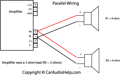
Wiring Diagram   Stereo on Series Wiring Involves Connecting The Amplifier S Positive Terminal To
Series Wiring Involves Connecting The Amplifier S Positive Terminal To.


Wiring Diagram   Stereo on Volvo 240dl Gl Radio Circuit And Wiring Diagram   Circuit Schematic
Volvo 240dl Gl Radio Circuit And Wiring Diagram Circuit Schematic.


Wiring Diagram   Stereo on Details Of 2002 Honda Civic Immobilizer System Circuit Diagram
Details Of 2002 Honda Civic Immobilizer System Circuit Diagram.


Wiring Diagram   Stereo on Subaru Legacy Cruise Control System Schematic Wiring Diagram
Subaru Legacy Cruise Control System Schematic Wiring Diagram.


Wiring Diagram   Stereo on 1996 Audi A4 Stereo Wiring By Eliana
1996 Audi A4 Stereo Wiring By Eliana.


Wiring Diagram   Stereo on Speaker Wiring Diagram Speaker Diagram Car Subwoofer Wiring Diagram
Speaker Wiring Diagram Speaker Diagram Car Subwoofer Wiring Diagram.


Dual Input Combining Stereo Line Amplifier

Posted by Unknown Monday, April 8, 2013 0 comments
This circuit takes two separate line-level stereo (L & R) signals and combines them into one stereo (L & R) output, thus avoiding the need to switch between two pairs of input signals. In the author’s application, it is used to feed the stereo audio from a TV receiver and a DVD player into an external amplifier. The need for the circuit arose because of a design peculiarity in the TV receiver. The TV has four A/V inputs and one A/V output. AV1-AV3 accept composite or S-video plus stereo audio inputs and these feed into the TV’s A/V output. AV4 accepts Component video (Y/Pb/Pr) plus stereo audio but unlike AV1-AV3, its audio (and video) signals are not fed to the TV A/V output. The Y/Pb/Pr input was chosen for use with the DVD player because of its superior video quality, while the audio was to be fed to an external amplifier for improved reproduction.
Circuit diagram:
stereo-line-amplifier-circuit-diagram
Dual Input-Combining Stereo Line Amplifier Circuit Diagram
However, manual switching was inconvenient, hence the genesis of this design. In use, the DVD player audio is fed in parallel to TV AV4 and to one input pair of the combining amplifier, while the TV audio output feeds the other input pair. The amplifier output goes to the external audio amplifier. There is no conflict between the two audio inputs because when AV4 (DVD player) is selected, there is no TV audio output. In all other modes, the DVD player is off. As shown, the circuit has a voltage gain of 1.5 times (3.5dB) but this can be altered as required by changing the two 15kW resistors. Input impedance is 10kW and the outputs are isolated from cable and amplifier input capacitance with 47W series resistors. The circuit can be powered from a regulated 12V DC plugpack.
Author: Garth Jenkinson - Copyright: Silicon Chip Electronics
Source : www.extremecircuits.net