Schematic | Circuit guide | Manual Wiring diagram | Electronic
Showing posts with label 1. Show all posts

1 Ma Current Sink Circuit Diagram

Posted by Unknown Thursday, December 26, 2013 0 comments
This is the simple 1-Ma Current Sink Circuit Diagram. A fixed current flows through any load that is connected between the positive supply and Ql`s collector. The non inverting terminal of the op amp is grounded, and negative feedback flows between the output of the circuit (Ql`s emitter) and the inverting terminal. The voltage across Rl is thus equal to the voltage at the inverting terminal (approximately 0.55 V), so a fixed current of about 1 mA flows through the load, Ql`s emitter, and Rl.


1-Ma Current Sink Circuit Diagram

1-Ma Current Sink Circuit Diagram

GENERATION OF 1 SEC PULSES SPACED 5 SEC APART

Posted by Unknown Monday, December 23, 2013 0 comments
        This circuit using a dual-timer NE556 can produce 1Hz pulses spaced 5 seconds apart, either manually or automatically. IC NE556 comprises two independent NE555 timers in a single package. It is used to produce two separate pulses of different pulse widths, where one pulse initiates the activation of the second pulse.


       The first half of the NE556 is wired for 5-second pulse output. When slide switch S2 is in position ‘a’, the first time is set for manual operation, i.e. by pressing switch S1 momentarily you can generate a single pulse of 5- second duration. When switch S2 is kept in ‘b’ position, i.e. pins 6 and 2 are shorted, timer 1 in NE556 triggers by itself.
         The output of the first timer is connected to trigger pin 8 of second timer, which, in turn, is connected to a potential divider comprising resistors R4 and R5. Resistor R1, preset VR1, resistor R2, preset VR2, and capacitors C2 and C5 are the components determining time period. Presets VR1 and VR2 permit trimming of the 5-second and 1-second pulse width of respective sections.
        When switch S2 is in position ‘a’ and switch S1 is pressed momentarily, the output at pin 5 goes high for about 5 seconds. The trailing (falling) edge of this 5- second pulse is used to trigger the second timer via 0.1μF capacitor C6. This action results in momentarily pulling down of pin 8 towards the ground potential, i.e. ‘low’. (Otherwise pin 8 is at 1/2 Vcc and triggers at/below 1/3 Vcc level.) When the second timer is triggered at the trailing edge of 5-second pulse, it generates a 1- second wide pulse.
         When switch S2 is on position ‘b’, switch S1 is disconnected, while pin 6 is connected to pin 2. When capacitor C is charged, it is discharged through pin 2 until it reaches 1/3Vcc potential, at which it is retriggered since trigger pin 6 is also connected here. Thus timer 1 is retriggered after every 5-second period (corresponding to 0.2Hz frequency). The second timer is triggered as before to produce a 1-second pulse in synchronism with the trailing edge of 5-second pulse.

1 W Home Stereo Amplifier Circuits Diagram

Posted by Unknown Tuesday, September 10, 2013 0 comments
This is a one watt home stereo amplifier module project using the KA2209 IC from Samsung, which is equivalent to the TDA2822. It operates from 3-12V DC & will work from a battery since the dormant current drain is low. It requires no heat sink for normal use. The input & output are both ground referenced. Maximum output will be obtained with a 12V power supply & 8 ohm speaker, however it is suitable for driving headphones from a supply as low as 3V.

The Specifications of the home stereo amplifier :

D.C. input : 3 – 12 V at 200 – 500 mA max
Idle current : approx. 10 mA
Power output : > 1 Watt max. 4-8 ohms, 12V DC
Freq. Resp. : approx. 40 Hz to 200 kHz, 8 ohm, G=10
THD : < 1 % @ 750 mW, 4-8 ohm, 12V
Gain : approx. x10 (20 dB) OR x100 (40dB)
S/N ratio : > 80 dB, G = 20 dB
Sensitivity : < 300 mV, G = 20 dB
Input Impedance : approx. 10 k ohm

Description 

The gain is adjustable from ten to 100, i.e. twenty to 40 dB. Start with feedback resistors R1 and R3 of 1k ohm, this will give a gain of ten which ought to be adequate for most applications. In case you need more gain, you can remove resistors R1 and R3.This will give a gain of about 100, or 40 dB.The input attenuation can be adjusted by the potentiometer which can be used as a volume control. The IC gain ought to be kept as low as necessary to accomplish full output, with the in put potentiometer and your signal source at maximum.

1 W Home Stereo Amplifier Circuit Diagram

1 W Home Stereo Amplifier


Voltage Gain = 1+ R1/R2 = 1+R3/R4, however the maximum gain with no outside feedback is about 100, or 40dB. (GdB = 20log Gv)

This will keep the signal to noise ratio as high as feasible. Additional gain provided by the amplifier will reduce the S/N ratio by a similar amount, since the input noise figure is constant. Other values for R1 and R3 of between 1k and 10k ohm can be used if an intermediate gain level is necessary.

If driving a pair of headphones, you may also need a 100 ohm resistor in series with each output to reduce the output level, depending on headphone impedance & sensitivity. Make positive you start with the volume right down to check. Numerous headphones may be driven from the amplifier in the event you wish, since most headphones have at least 16 ohm impedance, or more often 32 ohm.

There are only a few outside parts, the IC contains most of the necessary circuitry. R1,R2 and R3,R4 are the feedback resistors. C1 provides power supply decoupling. C2 and C3 are the input coupling capacitors, which block any DC that might-be present on the inputs. C4,C5 block DC in the feed back circuit from the inverting inputs, and C6,C7 are the output coupling capacitors. C8, R5 and C9,R6 act as Nobel networks providing a high frequency load to maintain stability at frequencies where loud speaker inductive reactant may become excessive. The pot provides adjustable input level attenuation.

1 W Home Stereo Amplifier parts list

Power Supply Variable 1 3V 12 2V 1A Circuit

Posted by Unknown Monday, August 12, 2013 0 comments
Power supply circuit to generate output below were variations between 1.3V DC to 12.2V DC with 1A current. In addition, the power supply circuit is also equipped with over-current protection or shield against belebih flow. Power supply circuit is very simple, but the quality is quite good, made her basiskan regulator IC LM723 is a pretty legendary.


1.3V DC to 12.2V DC Regulator Power Supply


Description:

R2 to set the output voltage. The maximum current is determined by R3, over-current protection circuit inside the LM723 to detect the voltage on R3, if it reaches 0.65 V, the voltage output will be off her. So the current through R3 can not exceed 0.65 / R3 although output short-circuit in his.


C3 and C4 are ceramic capacitors, as much as possible directly soldered to the PCB, this is because the LM723 is prone to oscillation that is not cool.


LM723 works with 9.5V input voltage to 40 V DC and the LM723 can generate its own current of 150mA when the output voltage is not more than 6-7V under input voltage.


Specifications:

Output (value estimated):


Vmin = (R4 + R5) / (R5 * 1.3)

Vmax = (7.15 / R5) * (R4 + R5)


Imax = 0.65/R3


Max. Power on R3: 0.42/R3


Min. DC Input Voltage (pin 12 to pin 7): Vmax + 5


Component List:

B1 40V/2.5A

C1 2200uF (3300uF even better)

C2 4.7uF

C3 100nF

C4 1NF

C5 330nF

C6 100uF

Green LED D1

D2 1N4003

F1 0.2A F

F2 2A M

IC1 LM723 (in a DIL14 plastic package)

R1 1k

R2 Pot. 5k

R3 0.56R/2W


R4 3.3k

R5 4.7k

S1 250V/1A

T1 2N3055 on a heatsink 5K / W

TR1 220V/17V/1.5

Make 5 1 Channel Audio Amplifier

Posted by Unknown Saturday, August 10, 2013 0 comments
5.1 channel amplifier consists of 6 amplifiers 1 channel mono, which has certain specifications on each canals. Has 6 channel surround sound amplifier that consists of Front Left ,Center,Front Right ,Rear Left (Left Surround),Rear Right (Right Surround) , and LFE (Subwoofer).For clarity I give a simple illustration of the layout and the circuit for these speakers.

5.1 Speaker Setup
5.1 Speaker Setup

Accoustic Field Generator
Acoustic Field Generator is generating acoustic sound with surround effects are adjustable with a standard Dolby Surround, able to produce surround sound is good enough but not too much need of funds. Technological developments as if not only focused on one area alone but on all fronts. The development of technologies that exist today one of them is in the field of audio. With more advanced audio technology today not only as mere entertainment but has become a hobby, hobby is not cheap of course. Many audio enthusiasts trying to make music sound that sounded to be very hard to make music sound as live, the addition of the amplifier, woofer or special speakers that cost is not cheap.

The sound effects are living seems to now is something that most do not have to exist in every good audio devices. This effect is basically a surround effect that can lead to sound as though coming from different directions and his voice can still be heard clearly. Currently Compo-tape tape that has been a lot of these facilities surround sound but not good enough when heard from a considerable distance because of the effects surroundnya missing. This is because the distance is too far listener and speaker, speaker layout is not quite right, or the effect of unfavorable surround.


Surround effects are nice and can be heard with a good surround system is a system that is in movie theaters and to make it not a bit prangkat needed funds. However, if satisfaction remains the number one then the fund is not a major problem. To find a middle ground between price and quality surround effects it was attempted to make the Acoustic Field Generator that can produce surround sound is good enough but not too much need of funds. Acoustic Field Generator is capable of generating acoustic sound with surround effects are adjustable with a standard Dolby Surround.
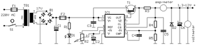

Accoustic Field Generator Construction

Basically an Acoustic Field Generator built from op-amp circuit and filters. Op-amps are usually used as a voltage amplifier in the Acoustic Field Generator is more widely used as active filters. The filter in the tool is very instrumental in creating an acoustic sound that is really clear, but in practice, almost all the filters, do not miss the precision of the signal with a specific frequency. An op-amp is good for this application is the op-amp which has a wide bandwidth, rise time, slew rate and fast setting timenya. In addition to op-amp and active filter, theres more important parts of the power supply. This is the part that is instrumental in creating excellence acoustic sound because of the bad power supply which is the only producer of noise, which will enter into a voice signal path so that should clear acoustic sound into an acoustic sound with the addition of reverberation (noise). The power supply used is the twin power supply + / - 18 volts DC. Part Acoustic Field Generators


Before we start doing this project, it helps us know in advance about the function of each speaker.


Front Channel

Channel Front is a forward channel input signal LR. LR signal is passed to an amplifier with gain = 1 so that this signal is passed without change / to filter the input signal LR. Front Left and Front Right, is a public speaker that we encountered in stereo amplifier, consisting of a woofer and tweeter. Woofers generally produce low tone sound with a frequency range ranging from 80Hz - 250Hz, while the tweeter produces a high tone with a frequency range between 15kHz - 20kHz. For projects that we will create, its good we use a good quality woofer, with a size of 10 inches and a type piezoelectric tweeter for each speaker fronts.


Front Channel 5.1 Amplifier


Center Channel

Center, the fullrange speakers, which produce sound with a frequency range between 80Hz - 10Khz. Output from the center speaker is a summation of left and right signal (left + right = center). In a movie or song Dolby Surround format, commonly used center for dialogue / vocal or speech of the actor / artist of a film and to produce a sound that moves ahead of us.


Center Channel 5.1 Amplifier


Rear Channel with Surround System

In this section is the core of this hard perangakat. These sections produce surround effects. To produce the surround effect is required special IC MN3005 / 8 and MN3101. Both these ICs will delay the incoming signal in several phases, so that the signal output from this phase will be left with a signal phase of the signal lain.Pada this section L and R are deducted (LR) and then passed in the buffer, filter LPF, delay line, filter LPF (7KHz) and the last is a splitter between the signals R and L. Circuit which causes the surround effect is 75KHz LPF circuit that produces its output fed to the Right Rear 75KHz LPF amplifier input while it diparalel with the Left Rear amplifier input so as to produce two signals L and R which is basically a LR signal a phase lag with the original signal phase.


Rear Left and Rear Right, also known as surround speakers. This speaker is generally a semi-midrange speaker (usually used on television or Mini Compo), commonly called satellite speakers. In a movie surround speakers are used to generate the audible sound of distant voices or sounds that move from the back of our approach. In a music surround speakers produce sound backing vocals and generally sounds like guitars, violins and trumpets sounded clear here.
Rear Channel 5.1 Amplifier


Subwoofer Channel

Part of this subwoofer is the summation of inputs L and R inputs to a summing amplifier. The output of the summing amplifier is passed to a class 2A LPF which will only pass signals with frequency rendah.Subwoofer, sometimes referred to as LFE (Low Frequency Effect). For these speakers using a subwoofer speaker. Speaker woofer speaker subwoofer is designed specifically to be able to respond to sound with a very low frequency, ranging from 15Hz - 120Hz. For low tone effect can be produced by either (without any harmonic frequency), then the acoustic box / box speakers are also designed specifically with a variety of methods (there are no visible speaker / inside the box, there are that use insulation / labyrinth, etc. ), so that the speaker is capable of compressing the air effectively, so that will feel the effect.

Subwoofer Channel 5.1 Amplifier


Wiring Diagram Home Theater Amplifier / 5.1 Amplifier


Adjustable 1 3 22V Regulated Power Supply

Posted by Unknown Wednesday, May 29, 2013 0 comments
Want a regulated voltage that can be adjusted to suit your application? This Adjustable Power Supply is small, easy to build and can be adapted to produce a fully regulated voltage ranging from 1.3V to 22V at currents up to 1A. This circuit come from SiliconChip Magazine

There are many fixed-voltage IC regulators available and these can be had with 5V, 6V 8V, 9V, 12V & 15V outputs. But what if you want a voltage output that does not fit into one of the standard ranges or if you want to be able to easily adjust this output voltage? An adjustable regulator is the answer – one that can be set to provide the exact voltage you require.

This Adjustable Power Supply comprises a small PC board that utilises a 3-terminal regulator. It does not have too many other components – in fact, there are just three diodes, three capacitors, a resistor and a trimpot to set the output voltage from the regulator. The circuit is based on an LM317T adjustable voltage regulator. D1 provides reverse polarity protection while P1 sets the output voltage.

Project looks like:
picture of the project
Picture Of The Project
Parts layout:
Parts layout of regulated power supply
Parts Layout Of The Project
PCB layout:
PCB layout for regulated power supply
PCB Layout Of The Project
Circuit diagram:
Adjustable 1.3-22V Regulated Power Supply
Adjustable Regulated DC Power Supply Circuit Diagram
Parts list:

IC = LM317T adjustable 3-terminal regulator
P1 = 2k horizontal trimpot
R1 = 110R-0.25W
C1 = 100uF-25V
C2 = 10uF-25V
C3 = 100uF-25V
D1 = 1N4004
D2 = 1N4004
D3 = 1N4004

LTC3588 1 Piezoelectric Energy Harvesting Power Supply Circuit

Posted by Unknown Monday, April 8, 2013 0 comments
Here’s a design circuit of The LTC3588-1 is a piezoelectric energy harvesting power supply IC that integrates a low-loss full-wave bridge rectifier with a high efficiency buck converter to form a complete energy harvesting solution optimized for high output impedance energy sources such as piezoelectric transducers. This is the figure of the circuit;


LTC3588-1 can be configured to deliver four output voltages: 1.8V, 2.5V, 3.3V and 3.6V. In this table you can see how you need to configure the pins of the LTC3588-1 to obtain the specified voltage.  To select Low for D0, D1 the pin must be connected to GND and if you need to select high for D0, D2 the pin must be connected to VIN2. The maximum output current can be set up to 100mA. As you can see in this power schematic circuit the design of power supply is very easy and require few external components. A power supply circuit based on the LTC3588-1 IC offers many features like: 950nA Input Quiescent Current (Output in Regulation – No Load) , 450nA Input Quiescent Current in UVLO, 2.7V to 20V Input Operating Range, Integrated Low-Loss Full-Wave Bridge Rectifier, Up to 100mA of Output Current, Selectable Output Voltages, High Efficiency Integrated Hysteretic Buck DC/DC.

The LTC3588-1 IC can be used in many applications circuits like: Piezoelectric Energy Harvesting, Electro-Mechanical Energy Harvesting, Wireless HVAC Sensors, Mobile Asset Tracking, Tire Pressure Sensors, Battery Replacement for Industrial Sensors, Remote Light Switches.

Power Supply Variable 1 3V 12 2V 1A Circuit

Posted by Unknown 0 comments
Power supply circuit to generate output below were variations between 1.3V DC to 12.2V DC with 1A current.
In addition, the power supply circuit is also equipped with over-current protection or shield against belebih flow. Power supply circuit is very simple, but the quality is quite good, made her basiskan regulator IC LM723 is a pretty legendary.


1.3V DC to 12.2V DC Regulator Power Supply


Description:

R2 to set the output voltage. The maximum current is determined by R3, over-current protection circuit inside the LM723 to detect the voltage on R3, if it reaches 0.65 V, the voltage output will be off her. So the current through R3 can not exceed 0.65 / R3 although output short-circuit in his.


C3 and C4 are ceramic capacitors, as much as possible directly soldered to the PCB, this is because the LM723 is prone to oscillation that is not cool.


LM723 works with 9.5V input voltage to 40 V DC and the LM723 can generate its own current of 150mA when the output voltage is not more than 6-7V under input voltage.


Specifications:

Output (value estimated):


Vmin = (R4 + R5) / (R5 * 1.3)

Vmax = (7.15 / R5) * (R4 + R5)


Imax = 0.65/R3


Max. Power on R3: 0.42/R3


Min. DC Input Voltage (pin 12 to pin 7): Vmax + 5


Component List:

B1 40V/2.5A

C1 2200uF (3300uF even better)

C2 4.7uF

C3 100nF

C4 1NF

C5 330nF

C6 100uF

Green LED D1

D2 1N4003

F1 0.2A F

F2 2A M

IC1 LM723 (in a DIL14 plastic package)

R1 1k

R2 Pot. 5k

R3 0.56R/2W


R4 3.3k

R5 4.7k

S1 250V/1A

T1 2N3055 on a heatsink 5K / W

TR1 220V/17V/1.5