Schematic | Circuit guide | Manual Wiring diagram | Electronic
Showing posts with label circuit. Show all posts

Touch Controlled Mute Switch Circuit Diagram

Posted by Unknown Friday, September 5, 2014 0 comments
Here is another simple circuit to mute the volume of Audio devices through simple touch. It exploits the action of the flip-flops in the timer IC 555 to reduce the volume of the Audio amplifier. IC NE555 is designed in the toggle mode. Its lower and upper comparator inputs are connected to the touch plates which can be membrane switches or two pieces of conducting plates. The inputs of comparators are stabilized through R1 and R2 to avoid floating.

Touch controlled Mute switch circuit diagram

 Touch Controlled Mute Switch Circuit Diagram

 
When the touch plate connected to pin 2 is touched momentarily, output of IC1 goes high and T1 conducts. The centre tap of the volume control is connected to the collector of T1. So when T1 conducts current going to the amplifier drains through T1. This reduces the volume.IC1 remains latched in this position with LED on. When the touch plate connected to pin 6 is touched momentarily, output of IC1 goes low and T1 turns off. This restores the volume.

Ultrasonic Mosquito Repeller Circuit Diagram by CD4017

Posted by Unknown Friday, December 27, 2013 0 comments
This is a simple ultrasonic mosquito repeller circuit diagram. The circuit is design on the theory that pests like mosquito can be repelled by ultrasonic frequency around (20KHz-25KHz). This ultrasonic mosquito repeller circuit is based on a single CMOS IC CD4017. C1,R1 & VR1 is used to adjust the output frequency.

Circuit Diagram:

Ultrasonic Mosquito Repeller Schematic
Fig: Ultrasonic mosquito repeller circuit diagram

1 Ma Current Sink Circuit Diagram

Posted by Unknown Thursday, December 26, 2013 0 comments
This is the simple 1-Ma Current Sink Circuit Diagram. A fixed current flows through any load that is connected between the positive supply and Ql`s collector. The non inverting terminal of the op amp is grounded, and negative feedback flows between the output of the circuit (Ql`s emitter) and the inverting terminal. The voltage across Rl is thus equal to the voltage at the inverting terminal (approximately 0.55 V), so a fixed current of about 1 mA flows through the load, Ql`s emitter, and Rl.


1-Ma Current Sink Circuit Diagram

1-Ma Current Sink Circuit Diagram

Circuit design tutorial in CircuitMaker 5

Posted by Unknown 0 comments
In this tutorial we are going to learn how to design and simulate a circuit schematic in CircuitMaker 5. For example we are going to design a 12V to 5V  dc-dc converter circuit diagram.  This is the circuit below that we are going to design. 

Fig-1: 12V to 5V  dc-dc converter circuit diagram


Let’s start design the circuit in circuitmaker 5.


Step-1: Open a new document.
Go to “File>New” as shown below or simply press “CTRL+N” 


This will opened a new workspace named as "UNTITLED.CKT(1)".As shown below...


Step-2: Device Selection.

Click on  “Parts”-(Use to display and select device) tool icon form tool bar. See below…

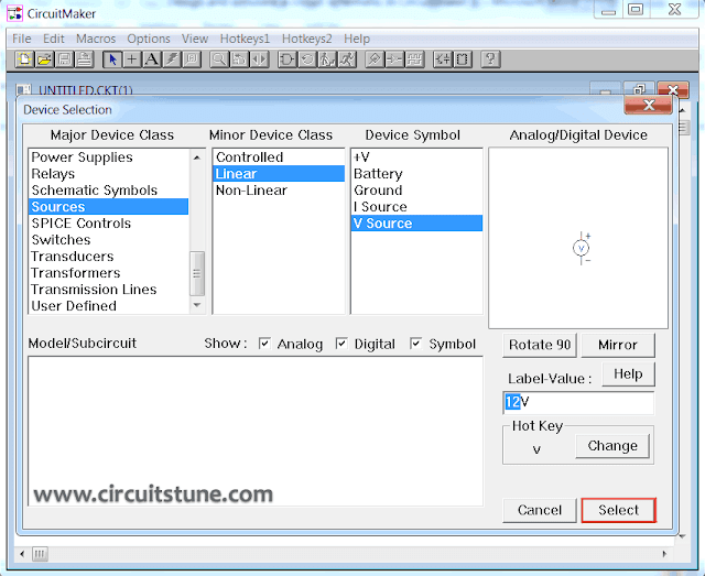
Or, simply hit on “x” from keyboard.This will bring up  “Device Selection” window.From this window select a 12V DC voltage soure by “Sources>Linear>V source” and change the voltage 10V to 12V as shown below.


After that click on “Select” or press “Enter”.

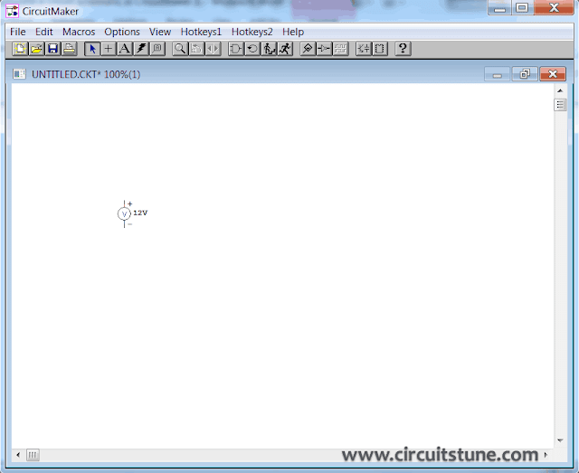
Now place the symbol where you like by left click on mouse .I placed here..


In the same way add a 78L05 regulator IC symbol. See below… 


And place it in workspace.


As same as add a Diode(shortcut key “d”), Capacitor(shortcut key “c”),and Ground(shortcut key “0”) symbol one after one in the same way and place in workspace(see below). To rotate  any device click on device and press “ALT+R”once or two times or as needed.


To see the circuit in zoom view press F2 . Then you see “Circuit Scale” window, enter a value between 10 to 2000 % that you want to scale (I’m entered 150%). And press “ENTER”.

Now the circuit symbol will larger, now we can design the circuit in circuitmaker 5 easily.


Back to adding schematic symbol.

Now add two “Terminal” (see below...)


Do that two times and then rotate as shown below.


Step-3: Connect the circuit.

Select the “Wire tool” (see below…) 


To connect two pins of two device click to pin(1) and drag until to pin(2). See below…

 
Connect all the pins that are necessary (see Fig:1).

After connect the circuit its looks something like this…


Step-4: Simulate the circuit using circuitmaker simulator.


Don’t worry, this is a simple task. But simulation is necessary for a circuit. To determine that it have any error or it giving us the expected output or not.

Before simulate the circuit we have to confirm that the simulation mode is Analog. To select Analog mode click once on “Digital/Analog” button from toolbar. And then the icon will change. See below...


Now click on “Run/Stop” button from toolbar. See below...


If a confirmation massages box come then select “Yes”.

Then you will see the simulation window. See below...

Showing input value of 12V to 5V  dc-dc converter circuit diagram
Showing output value of 12V to 5V  dc-dc converter circuit diagram
 
Note: If you want to change any parts/device/source value in the circuit, double click on the parts/device/source and enter your value.

We are all done and you can see in screenshot, the output voltage is 5V DC. And that is our expected output and circuit. If you want to know more about 12Vto 5V  dc-dc converter circuit then follow this link.

Thank you for reading. Have you faced any problem when trying to design the circuit and have I missed anything?

What you think? Should i post more tutorial about circuit design and CircuitMaker 5.

Build a Programmable Zener Circuit Diagram

Posted by Unknown Tuesday, December 24, 2013 0 comments
How to Build a Programmable Zener Circuit Diagram. The ICL8212 is connected as a programmable zener diode. Zener voltages from 2 V up to 30 V can be programmed by mostly suitable selecting R2. The zener voltage is: Because of the absence of internal compensation in the ICL8212, CI is necessary to ensure stability. 
 
Two points worthy of note are the extremely low-knee current (less than 300 ) and the low dynamic impedance (typically 4 to 7 ohms) over the operating current range of 300 to 12 mA. 

Programmable Zener Circuit Diagram

Programmable Zener Circuit Diagram

Shift Register Driver Power Supply Circuit Diagram

Posted by Unknown 0 comments
This is the Shift Register Driver Power Supply Circuit Diagram. A16 V power supply can be synthesized as shown using IN1692 rectifiers. A shift pulse input saturates the 2N2714 depriving the Darling-ton combination (2N2714 and 2N2868) of base drive.The negative pulse so generated on the 15 V line is differentiated to produce a positive trigger pulse at its trailing edge.

Shift Register Driver Power Supply Circuit Diagram

Shift Register Driver Power Supply Circuit Diagram

Simple Power Pulse Using by LM350 and NE555 Circuit Diagram

Posted by Unknown Friday, December 20, 2013 0 comments
This is a Simple Power Pulse Using by LM350 and NE555 Circuit Diagram. This circuit can use to drive lamp,power LED,DC motor etc. Adjust R5 for output amplitude.Adjust R1 for output power .

Power Pulse Circuit Diagram

Power Pulse Circuit Diagram


The LM350 is adjustable 3-terminal positive voltage regulators is capable of supplying in excess of 3A over a 1.2V to 33V output range.This circuit requires 5-15V power supply.

Build a Lcd Display Power Supply Circuit Diagram

Posted by Unknown Thursday, December 19, 2013 0 comments
This is the simple Lcd Display Power Supply Circuit Diagram. Laptop computers often use large-screen LCDs, which require a variable and a negative supply to ensure maximum contrast. This circuit operates from the system`s positive battery supply and generates a digitally variable negative voltage to drive the display. This figure`s switching regulator creates a negative voltage from the battery supply. The microprocessor data bus drives a 4-bit DAC, which in turn varies the actual regulator output from - 6.5 to -11.5 V. 

Lcd Display Power Supply Circuit Diagram


This arrangement allows a staircase of 16 possible voltages between these limits. The circuit implements the DAC by using the rail-to-rail output-drive capability of a 74 HC-series CMOS gate. A resistor divider network formed by the 240-kfi resistor, connected to the -V filter capacitor and the resistors, is referenced to the 5-V supply control (the MAX635 regulator). 

When the voltage at the VFb pin is greater than ground, the switching regulator turns on. The inductor dumps this energy into the -V filter capacitor. When the voltage at VFb is less than ground, the regulator skips a cycle. The MAX635 regulates the voltage at the junction of the resistor divider to 0 V. Thus, any resistor that the DAC connects to ground (logic 0) will not contribute any current to the ladder. Only the resistors that are at 5 V (logic 1) will be part of the voltage-divider equation. 

The entire switching-regulator supply draws less than 150 . You can place the circuit in an even lower power mode by interrupting the ground pin. The high-current path is from the battery input through the internal power PMOSFET to the external inductor. Disconnecting the ground connection simply disables the gate drive to the FET and turns off the internal oscillator.

Circuit Park Aid

Posted by Unknown Tuesday, October 8, 2013 0 comments
Three LEDs signal bumper-barrier distance, Infra-red operation, indoor use
This circuit was designed as an aid in parking the car near the garage wall when backing up. LED D7 illuminates when bumper-wall distance is about 20 cm., D7+D6 illuminate at about 10 cm. and D7+D6+D5 at about 6 cm. In this manner you are alerted when approaching too close to the wall. All distances mentioned before can vary, depending on infra-red transmitting and receiving LEDs used and are mostly affected by the color of the reflecting surface. Black surfaces lower greatly the device sensitivity. Obviously, you can use this circuit in other applications like liquids level detection, proximity devices etc.

Park-Aid Circuit DiagramParts:

R1_____________10K 1/4W Resistor
R2,R5,R6,R9_____1K 1/4W Resistors
R3_____________33R 1/4W Resistor
R4,R11__________1M 1/4W Resistors
R7______________4K7 1/4W Resistor
R8______________1K5 1/4W Resistor
R10,R12-R14_____1K 1/4W Resistors
C1,C4___________1µF 63V Electrolytic or Polyester Capacitors
C2_____________47pF 63V Ceramic Capacitor
C3,C5_________100µF 25V Electrolytic Capacitors
D1_____________Infra-red LED
D2_____________Infra-red Photo Diode (see Notes)
D3,D4________1N4148 75V 150mA Diodes
D5-7___________LEDs (Any color and size)
IC1_____________555 Timer IC
IC2___________LM324 Low Power Quad Op-amp
IC3____________7812 12V 1A Positive voltage regulator IC

Circuit operation:

IC1 forms an oscillator driving the infra-red LED by means of 0.8mSec. pulses at 120Hz frequency and about 300mA peak current. D1 & D2 are placed facing the car on the same line, a couple of centimeters apart, on a short breadboard strip fastened to the wall. D2 picks-up the infra-red beam generated by D1 and reflected by the surface placed in front of it. The signal is amplified by IC2A and peak detected by D4 & C4. Diode D3, with R5 & R6, compensates for the forward diode drop of D4. A DC voltage proportional to the distance of the reflecting object and D1 & D2 feeds the inverting inputs of three voltage comparators. These comparators switch on and off the LEDs, referring to voltages at their non-inverting inputs set by the voltage divider resistor chain R7-R10.

Circuit modification:

A circuit modification featuring an audible alert instead of the visual one is available here: Park-Aid Modification

Notes:
  • Power supply must be regulated (hence the use of IC3) for precise reference voltages. The circuit can be fed by a commercial wall plug-in adapter, having a DC output voltage in the range 12-24V.
  • Current drawing: LEDs off 40mA; all LEDs on 60mA @ 12V DC supply.
  • The infra-red Photo Diode D2, should be of the type incorporating an optical sunlight filter: these components appear in black plastic cases. Some of them resemble TO92 transistors: in this case, please note that the sensitive surface is the curved, not the flat one.
  • Avoid sun or artificial light hitting directly D1 & D2.
  • If your car has black bumpers, you can line-up the infra-red diodes with the (mostly white) license or number plate.
  • It is wiser to place all the circuitry near the infra-red LEDs in a small box. The 3 signaling LEDs can be placed far from the main box at an height making them well visible by the car driver.
  • The best setup is obtained bringing D2 nearer to D1 (without a reflecting object) until D5 illuminates; then moving it a bit until D5 is clearly off. Usually D1-D2 optimum distance lies in the range 1.5-3 cm.
  • If you are needing a simpler circuit of this kind driving a LED or a relay, click Infra-red Level Detector

LED Brake Rear Light Specifically for motorcycles Circuit diagram

Posted by Unknown Tuesday, October 1, 2013 0 comments
LEDs are used more and more in motor vehicles, replacing the standard incandescent lamps because they are more energy efficient and have a much longer life expectancy. In this article we describe a simple LED tail light that has been specifically designed for motorcycles, scooters and mopeds. There appears to be a significant need among motorcyclists for rear lights with LEDs, as evidenced by the many messages on this topic that turn up in various internet forums. The circuits that accompany these messages are often very rudimentary and therefore not very robust.

Mini project:


When designing an LED light for a motorcycle the following criteria need to be considered:

• Large variations of on-board voltage, this has a significant influence on light intensity.
• The circuit has to be (mechanically) robust.
• High light output is required (visibility = safety).
• Clearly visible difference in light intensity between rear light and brake light function.

After reading some of the literature concerning the use of LEDs in motor vehicles, it appears that the most common reason why LEDs still fail is the incorrect and/or insufficient use of series resistors.
In poorly implemented circuits there are often a number of LEDs connected in parallel which are all fed from a single series resistor. Because of small variations between LEDs, one LED can quickly give up the ghost. This causes an increase in current through the remaining LEDs and can easily lead to a domino effect, ultimately resulting in the failure of the entire circuit.With high-intensity LEDs, a small variation in current is immediately obvious as a large variation in light output.

This has to be taken into account when designing a circuit. This is important because when the engine rev speed goes up, the on-board voltage increases significantly. It would appear that you were braking when you actually opened the throttle instead.LEDs need mainly a constant current.That is why most circuits choose to drive LEDs from a constant-current source.

Circuit

This circuit has been designed to operate both as a motorcycle rear light and as a brake light. This requires two different currents. Because the voltages measured on the author’s motorcycle varied from 10.5 to 15 V and because two different currents are required for the total of 17 high-intensity LEDs it was not possible to use only one constant-current source.

Circuit diagram:

The idea was to turn the strongly varying DC voltage into a nice constant voltage first and then turn that into a constant current through a number of series resistors. The problem that is highlighted in many forums is the fact that the signal for the brake light is a positive voltage. It would require a lot of work on the motorcycle to change this. That is why the decision was made for a de sign that regulates the voltage on the chassis side, with the aid of a negative voltage regulator, a 7908. The disadvantage of this arrangement is that an additional chassis wire is required; normally the minus side of the lamps is directly connected to the chassis of the motorcycle.

However, the advantage is that both the + from the rear light as well as the + from the brake light can be directly connected to the LEDs.The ‘lamp’ con sists of a centre part with nine round, red,5-mm LEDs (HLMP EG08 Y200) wi th positioned around that eight oval ,r e d L E D s HLMP AD61 of 5 mm.The round LEDs D12 through D20 which have qui te a narrow radi ation angle are connected in series in sets of 3. Three of the se ‘strings’ are connected in parallel and each string has its own series resistor.

The oval LEDs D4 to D11 which have a wide radiation pattern are connected with two in series, so there are therefore four strings connected in parallel. These ensure with their wide radiation angle of 110 degrees that the rear/brake-light is also clearly visible from the side.The oval and round strings are connected to the brake contact via diodes. When the brake is operated all the strings are presented with the +12V from the battery via the series resistors. The light intensity therefore depends on the current that flows as a result of the series resistor (and the voltage drop across the diodes).

When the brake is not operated, the LEDs strings are still connected to the positive voltage of the battery, but this time via additional resistors R1 and R2.Because of the value of these resistors,the current is much lower and therefore also the light intensity. The intensity of the brake light can be adjusted using the series resistors (R3 to R9) in each of the individual strings,the brightness of the rear light is selected with the additional series resistors R1 and R2.Diode D1 has been added to protect the circuit from reverse connection of the power supply voltage.Electrolytic capacitors finally provide filtering for the fairly large varying,and not so clean, voltage.

The circuit was built into a silver coloured tube by the author. The electronics are mounted on two pieces of prototyping board, one behind the other,in the tube. The front (visible) PCB holds the LEDs and the series resistors. The LEDs are arranged as indicated next to the schematic. The 9 round LEDs are mounted in the middle of the rear light in a square pattern. The oval LEDs are mounted in a circle around the square.

The second PCB contains the remaining parts and the regulator.You can modify the circuit to your heart’s content by adding more strings, each fitted with its own diode and two resistors (a series resistor such as R3) and a resistor to +12 V (such as R1).The total current (when braking), must not exceed the maximum rating of the voltage regulator, this amounts to 1 A.

Author : Marcel Ulrich Copyright : elektor

A Bedside Lamp Timer Circuit Diagram

Posted by Unknown Sunday, September 29, 2013 0 comments

30 minutes operation, Blinking LED signals 6 last minutes before turn-off

The purpose of this circuit is to power a lamp or other appliance for a given time (30 minutes in this case), and then to turn it off. It is useful when reading at bed by night, turning off the bedside lamp automatically in case the reader falls asleep... After turn-on by P1 pushbutton, the LED illuminates for around 25 minutes, but then it starts to blink for two minutes, stops blinking for two minutes and blinks for another two just before switching the lamp off, thus signaling that the on-time is ending. If the user want to prolong the reading, he/she can earn another half-hour of light by pushing on P1. Turning-off the lamp at users ease is obtained by pushing on P2.

Circuit Diagram:

bedside 220 volt ac_lamp_timer schematic circuit  diagram

A Bedside Lamp Timer Circuit Diagram

Parts:
Resistors
R1 = 1K
R2 = 4K7
R3 = 10M
R4 = 1M
R5 = 10K

Capacitors
C1 = 470µF-25V
C2-C4100nF-63V

Semiconductors
C1 = 470µF-25V
C2-C4 = 100nF-63V
D1-D4 = 1N4002
D5 = 5mm. Red LED
IC1 = CD4012
IC2 = CD4060
Q1 = BC328
Q2 = BC547

Miscellaneous
P1,P2 = SPST Pushbuttons
T1 = 9+9 Volt Secondary 1VA Mains transformer
RL1 = 10.5V 470 Ohm Relay with SPDT 2A 220V switch
PL1 = Male Mains plug
SK1 = Female Mains socket

Circuit operation:

Q1 and Q2 form an ALL-ON ALL-OFF circuit that in the off state draws no significant current. P1 starts the circuit, the relay is turned on and the two ICs are powered. The lamp is powered by the relay switch, and IC2 is reset with a positive voltage at pin 12. IC2 starts oscillating at a frequency set by R4 and C4. With the values shown, pin 3 goes high after around 30 minutes, turning off the circuit via C3. During the c6 minutes preceding turn-off.

The LED does a blinking action by connections of IC1 to pins 1, 2 & 15 of IC2. Blinking frequency is provided by IC2 oscillator at pin 9. The two gates of IC1 are wired in parallel to source more current. If required, a piezo sounder can be connected to pins 1 & 14 of IC1. Obviously, timings can be varied changing C4 and/or R4 values.

Source : www.extremecircuits.net

PHONE BROADCASTER ELECTRONIC CIRCUIT DIAGRAM

Posted by Unknown Saturday, September 28, 2013 0 comments
PHONE BROADCASTER ELECTRONIC CIRCUIT DIAGRAM

The automatic switching consists of resistors R1-R3, variable resistor VR1 as the regulator, transistor T1 and T2, zener diode D2, and diode D1. R1 and VR1 is useful as an input voltage divider from the telephone line.

Parts list :

  •     Resistor R1-R2, R4 : 47k ohm
  •     Resistor R3 : 100 ohm
  •     Resistor R5 : 22k ohm
  •     Resistor R6 : 1M ohm
  •     VR1 : 100k ohm
  •     Diode D1 : 1N4001
  •     Zener diode D2 : 24V, 400mA
  •     Capacitor C1 : o.o1 uF
  •     Capacitor C2 : 330 pF
  •     Trimmer C3 : 50p
  •     Capacitor C4 : 5.6 pF
  •     Capacitor C5 : 10 pF
  •     Transistor T1-T2 : BC548
  •     Transistor T3 : BF494
  •     Inductor L1 : 45rotation 36SWG in resistor carbon 1M 1W
  •     Inductor L2 : 3 rotation 21 SWG 12mm diameter
  •     Antenna

A Simple NiCd Charger Circuit Diagram

Posted by Unknown Friday, September 27, 2013 0 comments
A simple NiCd charger can be built using ‘junk box’ components and an inexpensive LM317 or 78xx voltage regulator. Using a current limiter composed of R3 and a transistor, it can charge as many cells as desired until a ‘fully charged’ voltage determined by the voltage regulator is reached, and it indicates whether it is charging or has reached the fully charged state. If the storage capacitor (C1) is omitted, pulsed charging takes place. In this mode, a higher charging current can be used, with all of the control characteristics remaining the same.
The operation of the circuit is quite simple. If the cells are not fully charged, a charging current flows freely from the voltage regulator, although it is limited by resistor R3 and transistor T1. The limit is set by the formula Imax ≈ (0.6 V) ÷ R3 For Imax = 200 mA, this yields R3 = 3 Ω. The LED is on if current limiting is active, which also means that the cells are not yet fully charged. The potential on the reference lead of the voltage regulator is raised by approximately 2.9 V due to the voltage across the LED.
Circuit Diagram :
A Simple Nicd Charger Circuit Diagram
This leads to a requirement for a certain minimum number of cells. For an LM317, the voltage between the reference lead and the output is 1.25 V, which means at least three cells must be charged (3 × 1.45 V > 2.9 V + 1.25 V). For a 78xx with a voltage drop of around 3 V (plus 2.9 V), the minimum number is four cells. When the cells are almost fully charged, the current gradually drops, so the current limiter becomes inactive and the LED goes out.
In this state, the voltage on the reference lead of the regulator depends only on voltage divider R1/R2. For a 7805 regulator, the value of R2 is selected such that the current through it is 6 mA. Together with the current through the regulator (around 4 mA), this yields a current of around 10 mA through R1. If the voltage across R1 is 4 V (9 V – 5 V), this yields a value of 390 Ω. The end-of-charge voltage can thus be set to approximately 8.9 V. As the current through the regulator depends on the device manufacturer and the load, the value of R1 must be adjusted as necessary. The value of the storage capacitor must be matched to the selected charging current. As already mentioned, it can also be omitted for pulse charging.
Author: Wolfgang Schmidt   Copyright: Elektor

On Off Touch Switch Circuit Digram

Posted by Unknown Wednesday, September 25, 2013 0 comments
Small and portable unit, Suitable for normal-type devices
The modern mechanic switches are improved concerning of old technology. We need however many times to replacement some old switch or to check currents bigger than the durability of certain switches or simple we need something with modern appearance. For he and different reasons is essential the up circuit. It is simple in the manufacture and the materials that use they exist everywhere.
Circuit diagram:
On-Off_Touch_Switch_Circuit digram
Parts:
R1 = 3.3M
R2 = 3.3M
R3 = 10K
R4 = 1K
C1 = 10nF-63V
D1 = 1N4007
D2 = Red LED
Q1 = BC547
IC1 = NE555
RL1 = 12V Relay
Circuit Operation:
This circuit is based on the well known timer IC 555 (IC1), which drives a relay of which the contacts play the role of switch. The metal surfaces can have what form we want, but it should they are clean and near in the circuit. In order to it changes situation it suffices touch soft somebody from the two plates. Plate MP1 in order to the contacts of RL1 close [ON], or plate MP2 in order to the contacts of RL1 open [OFF]. The current that RL1 will check depended from his contacts. The Led D2 turns on when the switch they are in place ON and the contacts of RL1 closed. Two small pieces of metal can be used instead of MP1 – MP2. Because MP = Metal Plate.

Over voltage Protection Circuit Diagram

Posted by Unknown Wednesday, September 11, 2013 0 comments
When testing a circuit, a source of voltage that is variable and has over voltage shutdown is veiy useful. In this circuit, Rl is adjusted to 1 to 2 V below the eventual shutdown threshold. R2 sets the trip voltage. When this voltage is reached, the circuit shuts the voltage to the circuit under test down. To reset, reduce Rl below trip threshold and depress reset switch SI.

Over voltage Protection Circuit Diagram

Overvoltage Protection Circuit Diagram

Car Battery Charger Circuit

Posted by Unknown Wednesday, September 4, 2013 0 comments
Description
This charger will quickly and easily charge most any lead acid battery. The charger delivers full current until the current drawn by the battery falls to 150 mA. At this time, a lower voltage is applied to finish off and keep from over charging. When the battery is fully charged, the circuit switches off and lights a LED, telling you that the cycle has finished.
Circuit Diagram
Parts
R1 500 Ohm 1/4 W Resistor
R2 3K 1/4 W Resistor
R3 1K 1/4 W Resistor
R4 15 Ohm 1/4 W Resistor
R5 230 Ohm 1/4 W Resistor
R6 15K 1/4 W Resistor
R7 0.2 Ohm 10 W Resistor
C1 0.1uF 25V Ceramic Capacitor
C2 1uF 25V Electrolytic Capacitor
C31000pF 25V Ceramic Capacitor
D1 1N457 Diode
Q1 2N2905 PNP Transistor
U1 LM350 Regulator
U2 LM301A Op Amp
S1Normally Open Push Button Switch
MISC Wire, Board, Heatsink For U1, Case, Binding Posts or Alligator Clips For Output
Notes
1. The circuit was meant to be powered by a power supply, which is why there is no transformer, rectifier, or filter capacitors on the schematic. There is no reason why you cannot add these.
2. A heatsink will be needed for U1.
3. To use the circuit, hook it up to a power supply/plug it in. Then, connect the battery to be charged to the output terminals. All you have to do now is push S1 (the "Start" switch), and wait for the circuit to finish.
4. If you want to use the charger without having to provide an external power supply, use the following circuit.
 Circuit Diagram

C1 6800uF 25V Electrolytic Capcitor
T1 3A 15V Transformer
BR1 5A 50V Bridge Rectifier 10A 50V Bridge Rectifier
S1 5A SPST Switch
F1 4A 250V Fuse
5. The first time you use the circuit, you should check up on it every once and a while to make sure that it is working properly and the battery is not being over charged.
Author:
Source: http://www.aaroncake.net

Lithium Polymer Peak Charger Circuit Diagram

Posted by Unknown Monday, September 2, 2013 0 comments
Description
This circuit was developed to charge the Lithium-Polymer cells used in a model aircraft. Lithium-Polymer cells are incredibly lightweight compared to Ni-cad battery packs of the same voltage and amp-hour rating. Their only drawback is that they require a rigid charge and discharge regime to achieve maximum life. The most important points of note are as follows:
Circuit Diagram:

  1. They should be charged using a constant-current, constant-voltage method, which stops the charge once the current has dropped to about the C/10 rate. For example, for an 800mAh pack, charging should be terminated once the current falls to approximately 80mA.
  2. They should never be discharged below 3V per cell otherwise they will be permanently damaged.
  3. should not be charged or discharged above their rated current otherwise an explosion and fire can result!
To initiate charging, the momentary "Start" button (switch S1) is pressed, closing the relay contacts and connecting the battery pack to the output of REG1. The circuit will then charge two 800mAh cells in series at a constant current of 600mAh until they reach a peak terminal voltage of 4.2V per cell (nominal terminal voltage for these cells is 3.7V).
REG1 and transistor Q2 form a current-limited voltage regulator. When the charge current exceeds about 600mA, the voltage developed across R7 turns on Q2, which in turn pulls the adjust terminal of REG1 towards ground. This shunts the voltage adjustment resistance chain formed by VR2 and R3, thereby limiting the output to 600mA.
When the battery voltage reaches about 8.4V, the regulator limits any further voltage increase, as set by VR2. The charge current will then slowly decrease as the cells reach full capacity. As a result, the voltage across R7 also falls, until the bias voltage on the base of Q1 is too small to keep it in conduction. When Q1 turns off, the relay also turns off, isolating the fully charged battery.
The charger is set up as follows:
  1. It to 12V DC and place a digital voltmeter between the output of REG1 and the negative output for the battery pack. Adjust VR2 for a reading of 8.4V.
  2. VR1 so that the voltage on the base of Q1 is at maximum.
  3. Place an ammeter in series with the battery to be charged and press the "Start" button. The output current will shoot up to around 600mA, then slowly decrease over the next one to two hours.
Once it falls to around 80mA (or whatever the C/10 rate is for your cells), slowly turn VR1 until the relay switches off and indicator LED goes out.
The circuit should now charge your battery packs to within 97% of their rated capacity.
Finally, note that in most cases, REG1 will need to be fitted with a heatsink.
 Source - Silicon Chip January 2005

AC Line Current Detector Circuit

Posted by Unknown Sunday, September 1, 2013 0 comments
Circuit Diagram 
Desription
This circuit will detect AC line currents of about 250 mA or more without making any electrical connections to the line. Current is detected by passing one of the AC lines through an inductive pickup (L1) made with a 1 inch diameter U-bolt wound with 800 turns of #30 - #35 magnet wire. The pickup could be made from other iron type rings or transformer cores that allows enough space to pass one of the AC lines through the center. Only one of the current carrying lines, either the line or the neutral should be put through the center of the pickup to avoid the fields cancelling. I tested the circuit using a 2 wire extension cord which I had separated the twin wires a small distance with an exacto knife to allow the U-bolt to encircle only one wire.
The magnetic pickup (U-bolt) produces about 4 millivolts peak for a AC line current of 250 mA, or AC load of around 30 watts. The signal from the pickup is raised about 200 times at the output of the op-amp pin 1 which is then peak detected by the capacitor and diode connected to pin 1. The second op-amp is used as a comparator which detects a voltage rise greater than the diode drop. The minimum signal needed to cause the comparator stage output to switch positive is around 800 mV peak which corresponds to about a 30 watt load on the AC line. The output 1458 op-amp will only swing within a couple volts of ground so a voltage divider (1K/470) is used to reduce the no-signal voltage to about 0.7 volts. An additional diode is added in series with the transistor base to ensure it turns off when the op-amp voltage is 2 volts. You may get a little bit of relay chatter if the AC load is close to the switching point so a larger load of 50 watts or more is recommended. The sensitivity could be increased by adding more turns to the pickup.
Source - http://www.bowdenshobbycircuits.info/page8.htm#aclatch.gif

Simple Portable Amplifier Circuit Diagram

Posted by Unknown Thursday, August 15, 2013 0 comments
Simple Portable Amplifier Circuit Diagram Ul, an FET op amp needs a bipolar voltage atpins 4 and 7 with a common ground for optimum gain. You can calculate the gain by dividing R2 by Rl. Zero-set balance can be had through pins i and 5 through R3. Put a voltmeter between pin 6 and ground and adjust R3 for zero voltage. Once you`ve established that, you can measure the ohmic resistance at each side of R3`s center tap and replace the potentiometer with fixed resistors. R6, R7, RS,and C3 forrn a tone control that will give you added bass boost, if needed

Simple Portable Amplifier Circuit Diagram


Simple Portable Amplifier Circuit Diagram

Build a Variable Frequency Audio Band pass Filter Circuit Diagram

Posted by Unknown Wednesday, August 14, 2013 0 comments
This variable-frequency, audio bandpass filter is built around two 741 op amps that are connected in cascade. Two 741 op amps are configured as identical RC active filters and are connected in cascade for better selectivity. The filter`s tuning range is from 500~Hz to 1500 Hz. The overall voltage gain is slightly greater than 1 and the filter`s is about 5, The circuit can handle input signals of 4 V peak-to-peak without being overdriven. The circuit`s input impedance is over 200 kohm and its output impedance is less than 1 kohm

Variable-Frequency Audio Bandpass Filter Circuit Diagram

Variable-Frequency Audio Bp Filter Circuit Diagram