Schematic | Circuit guide | Manual Wiring diagram | Electronic
Showing posts with label a. Show all posts

Build a Programmable Zener Circuit Diagram

Posted by Unknown Tuesday, December 24, 2013 0 comments
How to Build a Programmable Zener Circuit Diagram. The ICL8212 is connected as a programmable zener diode. Zener voltages from 2 V up to 30 V can be programmed by mostly suitable selecting R2. The zener voltage is: Because of the absence of internal compensation in the ICL8212, CI is necessary to ensure stability. 
 
Two points worthy of note are the extremely low-knee current (less than 300 ) and the low dynamic impedance (typically 4 to 7 ohms) over the operating current range of 300 to 12 mA. 

Programmable Zener Circuit Diagram

Programmable Zener Circuit Diagram

When looking for a quality laser pointer

Posted by Unknown Sunday, December 22, 2013 0 comments
When looking for a quality laser pointer, the first thing that you should do is to ask yourself on what standards of quality you are looking for in such products. Many people want a pointer that will last for a long time. This means that they will no longer be bothered by always changing the device. Aside from that, having a quality product that will give quality results for a long time can actually save you money. If you want to be sure about the quality of the laser pointer that you are going to buy, you have to do a simple research about the products. It is not about what the manufacturers say about the product but it is about what the customers say about it.

Laser pointers of today are truly amazing. With such design and features that are really high-technology, there is no way that you will not buy if you can afford it. In fact, many people already have this device especially when they really need it in their work or industry. So if you think you want to be cool by having this device, this is your opportunity to have it and show it off to your friends.

But remember, you have to also be careful in using this for it can be hazardous without following its safety instructions.I can still remember my first laser pointer when I was in college. I was a prankster then and I used to make my classmates laugh by pointing it in the forehead of my teacher and the class started to laugh. Good thing that teacher was telling corny jokes and he was amazed that many of us laughed. He was unaware that we were not laughing at his joke but at the red dot seen on his head. Yes, the pointers available then were only red. But now, you can choose from various colors available.

Going back to the uses of these laser products, many people are benefiting from the light that it gives nowadays. The intensity of the light emitted by these products is brighter than before where they can go on a frequency up to 532nm. In fact, this is the fastest selling today can beam up to 80 miles reach. That can be an awesome ability that a pointer can give. It means that the light is intense that it can even burn easily combustible materials such as dry paper. In those years of its development, many professionals and students have been using this little piece of laser technology. It is typically used as a pointer in presentations and lectures. Aside from that, they are also used in night adventures, researches, and more.

Build a Lcd Display Power Supply Circuit Diagram

Posted by Unknown Thursday, December 19, 2013 0 comments
This is the simple Lcd Display Power Supply Circuit Diagram. Laptop computers often use large-screen LCDs, which require a variable and a negative supply to ensure maximum contrast. This circuit operates from the system`s positive battery supply and generates a digitally variable negative voltage to drive the display. This figure`s switching regulator creates a negative voltage from the battery supply. The microprocessor data bus drives a 4-bit DAC, which in turn varies the actual regulator output from - 6.5 to -11.5 V. 

Lcd Display Power Supply Circuit Diagram


This arrangement allows a staircase of 16 possible voltages between these limits. The circuit implements the DAC by using the rail-to-rail output-drive capability of a 74 HC-series CMOS gate. A resistor divider network formed by the 240-kfi resistor, connected to the -V filter capacitor and the resistors, is referenced to the 5-V supply control (the MAX635 regulator). 

When the voltage at the VFb pin is greater than ground, the switching regulator turns on. The inductor dumps this energy into the -V filter capacitor. When the voltage at VFb is less than ground, the regulator skips a cycle. The MAX635 regulates the voltage at the junction of the resistor divider to 0 V. Thus, any resistor that the DAC connects to ground (logic 0) will not contribute any current to the ladder. Only the resistors that are at 5 V (logic 1) will be part of the voltage-divider equation. 

The entire switching-regulator supply draws less than 150 . You can place the circuit in an even lower power mode by interrupting the ground pin. The high-current path is from the battery input through the internal power PMOSFET to the external inductor. Disconnecting the ground connection simply disables the gate drive to the FET and turns off the internal oscillator.

Petrol Gas Switch For A Pajero

Posted by Unknown Monday, October 7, 2013 0 comments

My current vehicle, a Pajero, was modified for dual fuel - ie, petrol and gas. However, its necessary to run the vehicle on petrol at regular intervals to stop the injectors from clogging up. This simple circuit allows the vehicle to be started using petrol and then automatically switches it to gas when the speed exceeds 45km/h and the brake pedal is pressed. Alternatively, the vehicle may be run on petrol simply by switching the existing petrol/gas switch to petrol. You can also start the vehicle on gas by pressing the brake pedal while starting the vehicle. The circuit is based on an LM324 dual op amp, with both op amps wired as comparators. It works like this: IC1a buffers the signal from the vehicles speed sensor and drives an output filter network (D1, a 560kO resistor and a 10µF capacitor) to produce a DC voltage thats proportional to the vehicles speed.

Circuit diagram:

petrol-gas-switch-for-a-pajero Circuit

This voltage is then applied to pin 5 of IC1b and compared with the voltage set by trimpot VR1. When pin 7 of IC1b goes high, transistor Q1 turns on. This also turns on transistor Q2 when the brake pedal is pressed (pressing the brake pedal applies +12V from the brake light circuit to Q2s emitter). And when Q2 turns on, relay 1 turns on and its contacts switch to the gas position. Trimpot VR1 must be adjusted so that IC1bs pin 7 output switches high when the desired trigger speed is reached (ie, 45km/h). In effect, the speed signal is ANDed with the brake light signal to turn on the relay. The vehicle has been running this circuit for several years now and is still running well, with no further injector cleans required.

Author: J. Malnar - Copyright: Silicon Chip Electronics

Source : www.extremecircuits.net

A Bedside Lamp Timer Circuit Diagram

Posted by Unknown Sunday, September 29, 2013 0 comments

30 minutes operation, Blinking LED signals 6 last minutes before turn-off

The purpose of this circuit is to power a lamp or other appliance for a given time (30 minutes in this case), and then to turn it off. It is useful when reading at bed by night, turning off the bedside lamp automatically in case the reader falls asleep... After turn-on by P1 pushbutton, the LED illuminates for around 25 minutes, but then it starts to blink for two minutes, stops blinking for two minutes and blinks for another two just before switching the lamp off, thus signaling that the on-time is ending. If the user want to prolong the reading, he/she can earn another half-hour of light by pushing on P1. Turning-off the lamp at users ease is obtained by pushing on P2.

Circuit Diagram:

bedside 220 volt ac_lamp_timer schematic circuit  diagram

A Bedside Lamp Timer Circuit Diagram

Parts:
Resistors
R1 = 1K
R2 = 4K7
R3 = 10M
R4 = 1M
R5 = 10K

Capacitors
C1 = 470µF-25V
C2-C4100nF-63V

Semiconductors
C1 = 470µF-25V
C2-C4 = 100nF-63V
D1-D4 = 1N4002
D5 = 5mm. Red LED
IC1 = CD4012
IC2 = CD4060
Q1 = BC328
Q2 = BC547

Miscellaneous
P1,P2 = SPST Pushbuttons
T1 = 9+9 Volt Secondary 1VA Mains transformer
RL1 = 10.5V 470 Ohm Relay with SPDT 2A 220V switch
PL1 = Male Mains plug
SK1 = Female Mains socket

Circuit operation:

Q1 and Q2 form an ALL-ON ALL-OFF circuit that in the off state draws no significant current. P1 starts the circuit, the relay is turned on and the two ICs are powered. The lamp is powered by the relay switch, and IC2 is reset with a positive voltage at pin 12. IC2 starts oscillating at a frequency set by R4 and C4. With the values shown, pin 3 goes high after around 30 minutes, turning off the circuit via C3. During the c6 minutes preceding turn-off.

The LED does a blinking action by connections of IC1 to pins 1, 2 & 15 of IC2. Blinking frequency is provided by IC2 oscillator at pin 9. The two gates of IC1 are wired in parallel to source more current. If required, a piezo sounder can be connected to pins 1 & 14 of IC1. Obviously, timings can be varied changing C4 and/or R4 values.

Source : www.extremecircuits.net

A Simple NiCd Charger Circuit Diagram

Posted by Unknown Friday, September 27, 2013 0 comments
A simple NiCd charger can be built using ‘junk box’ components and an inexpensive LM317 or 78xx voltage regulator. Using a current limiter composed of R3 and a transistor, it can charge as many cells as desired until a ‘fully charged’ voltage determined by the voltage regulator is reached, and it indicates whether it is charging or has reached the fully charged state. If the storage capacitor (C1) is omitted, pulsed charging takes place. In this mode, a higher charging current can be used, with all of the control characteristics remaining the same.
The operation of the circuit is quite simple. If the cells are not fully charged, a charging current flows freely from the voltage regulator, although it is limited by resistor R3 and transistor T1. The limit is set by the formula Imax ≈ (0.6 V) ÷ R3 For Imax = 200 mA, this yields R3 = 3 Ω. The LED is on if current limiting is active, which also means that the cells are not yet fully charged. The potential on the reference lead of the voltage regulator is raised by approximately 2.9 V due to the voltage across the LED.
Circuit Diagram :
A Simple Nicd Charger Circuit Diagram
This leads to a requirement for a certain minimum number of cells. For an LM317, the voltage between the reference lead and the output is 1.25 V, which means at least three cells must be charged (3 × 1.45 V > 2.9 V + 1.25 V). For a 78xx with a voltage drop of around 3 V (plus 2.9 V), the minimum number is four cells. When the cells are almost fully charged, the current gradually drops, so the current limiter becomes inactive and the LED goes out.
In this state, the voltage on the reference lead of the regulator depends only on voltage divider R1/R2. For a 7805 regulator, the value of R2 is selected such that the current through it is 6 mA. Together with the current through the regulator (around 4 mA), this yields a current of around 10 mA through R1. If the voltage across R1 is 4 V (9 V – 5 V), this yields a value of 390 Ω. The end-of-charge voltage can thus be set to approximately 8.9 V. As the current through the regulator depends on the device manufacturer and the load, the value of R1 must be adjusted as necessary. The value of the storage capacitor must be matched to the selected charging current. As already mentioned, it can also be omitted for pulse charging.
Author: Wolfgang Schmidt   Copyright: Elektor

Build a Cell Phone Jammer Schematic Diagram

Posted by Unknown Wednesday, September 11, 2013 0 comments
Build a Cell Phone Jammer Schematic Diagram
 
This cell phone jammer operates at GSM800 frequency since most mobile phones use it to operate. So the selected VCO is a sweeping oscillator, which is very effective but may be hard to construct for the beginners without nice RF-testing equipment.

As a noise source you can use 45MHz clock oscillator which is driving Local Oscillator port located on a mini-circuit mixer. There is also an impedance matching network for Local Oscillator signal to pass through it. It is used to equate impedances of the clock oscillator and the port of the mixer.

RF input (which is this port of the mixer) connected to the first 800MHz cell phone antenna, and the RF output is sent to the mini-circuit amplifier. This amplifier increases the output power for 15-16dbm. The amplified signal then sent to the second cell phone antenna.

Build a Cell Phone Jammer Schematic Diagram


 works
All cell phones which use GSM800 have their transmitted and received frequencies always separated by 45MHz. So when the mobile phone tries to call it is blocked by its own signal returning to it! Isn’t that cool? When the phone blabber annoys you – turn your jammer on and that wrongdoer will hear own voice in his or her cell phone.

Oh, by the way, you can also use this mobile signal jammer to block any cell-based tracking systems which use your GPS to track and record your car’s moves. And it is quite possible (though I didn’t actually tested it) to jam IEDs which detonated using cell phones.

Build a Cell Phone Jammer Schematic Diagram


The mixer used is designed to work up to 600MHz but in this case it works pretty well.

Build a Cell Phone Jammer Schematic Diagram
 
RF amplifier is doing its job perfectly yet (as it was mentioned in the Jammer Store blog post) draws additional power.Old aluminium box was used as a frame for the jammer and old UHF connectors from Motorola cell phone as input/output.You need to attach RF connectors to the circuit. Nine volt battery and voltage regulator were used to supply all components. The battery was placed inside and separated by the foamed plastic from the other components.The power on/off switch is placed on the top. The input and output antennas (also from old Motorola mobile phone) are screwed onto UHF connectors.Your cell phone jammer is ready. Enjoy!

Build a Cell Phone Jammer Schematic Diagram


Build a Variable Frequency Audio Band pass Filter Circuit Diagram

Posted by Unknown Wednesday, August 14, 2013 0 comments
This variable-frequency, audio bandpass filter is built around two 741 op amps that are connected in cascade. Two 741 op amps are configured as identical RC active filters and are connected in cascade for better selectivity. The filter`s tuning range is from 500~Hz to 1500 Hz. The overall voltage gain is slightly greater than 1 and the filter`s is about 5, The circuit can handle input signals of 4 V peak-to-peak without being overdriven. The circuit`s input impedance is over 200 kohm and its output impedance is less than 1 kohm

Variable-Frequency Audio Bandpass Filter Circuit Diagram

Variable-Frequency Audio Bp Filter Circuit Diagram
 

1994 Volvo 850 Turbo Change the ECU with A Non Turbo ECU Parts

Posted by Unknown Wednesday, August 7, 2013 0 comments


When the ecu of my 1994 Volvo 850 Turbo was showing some bad readings about the knock sensors, I picked and pulled the old ecu and got a new ecu from a 1993 volvo 850 non turbo. Is it possible for an ECU from a turbo car to replace ecu from a non turbo car? Thanks.

Answer: No. The turbo creates a significant change, since the engine compression is changed significantly. 
VVT
A/F Ratio
Wastegate control
Banked injection
Would be different or missing from the ECU. The knock sensor sends signals when the A/F mixture pre-detonates before it can be ignited by the spark plug, and the computer corrects it with VVT. You need to buy the correct ECU.

Build a high volt supply Circuit Diagram

Posted by Unknown Sunday, August 4, 2013 0 comments
A light dimmer, a 1 µf capacitor and a 12 V car ignition coil form the simple line powered HV generator. The current in the dimmer is shown in Fig. B. At times tp t2, set by the dimmer switch, the inner triac of the dimmer switches on, and a very high and very fast current pulse charges the capacitor through the primary of the induction coil. 

Then at a rate of 120 times per second for a 60 Hz line, a very high voltage pulse appears at the secondary of the coil. To obtain an HV dc output, use a voltage doubler. Dl and D2 are selenium rectifiers (TV 18 Siemens or ITT) used for the supply of television sets. High value output shock protection resistors, R, are recommended when suitable. 

 Build a high-volt supply Circuit Diagram

Build a high-volt supply Circuit Diagram

How to Build a Dual Axis Solar Tracker System Mechanism and Control Circuit Explained

Posted by Unknown Sunday, May 26, 2013 0 comments

The circuit and the mechanism explained in this article may be considered as the easiest and perfect dual axis solar tracker system. 

The device is able to track the daytime motion of the sun precisely and shift in the vertical axis accordingly.

 The device also effectively tracks the seasonal displacement of the sun and moves the entire mechanism in the horizontal plane or in a lateral motion such that the orientation of the solar panel is always kept in a straight axis to the sun so that it complements the vertical actions of the tracker appropriately.


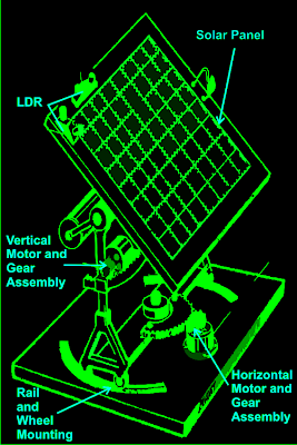
As shown in the figure, a relatively easy mechanism can be witnessed here. The solar tracker is basically mounted over a couple of stand with a central movable axis.

The pivotal arrangement allows the panel mounts to move on a circular axis over almost 360 degrees.

A motor gear mechanism as shown in the diagram is fitted just at the corner of the pivotal axis in such a way that when the motor rotates the entire solar panel shifts proportionately about its central pivot, either anticlockwise or clockwise, depending upon the motion of the motor which in turn depends on the position of the sun.

The position of the LDRs are critical here and the set of LDR which corresponds to this vertical plane movement is so positioned that it senses the sun light accurately and tries to keep the panel perpendicular to the sun rays by moving the motor in the appropriate direction through a definite number of stepped rotations.

The LDR sensing is actually accurately received and interpreted by an electronic circuit which commands the motor for the above explained actions.

Another mechanism which is quite similar to the above vertical setting, but moves the panel through a lateral motion or rather it moves the whole solar panel mount in circular motion over the horizontal plane.

This motion takes place in response to the position of the sun during the seasonal changes, therefore in contrast to the vertical movements; this operation is very gradual and cannot be experienced on a daily basis.

Again the above motion is in response to the command given to the motor by the electronic circuit which operates in response to the sensing done by the LDRs.

For the above procedure a different set of LDRs are used and are mounted horizontally over the panel, at a specific position as shown in the diagram.

How the Solar Tracker Control Circuit Functions

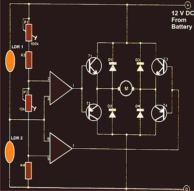
A careful investigation of the circuit shown in the diagram reveals that the whole configuration is actually very simple and straightforward. Here a single IC 324 is utilized and only two of its op amps are employed for the required operations.

The op amps are primarily wired to form a kind of window comparator, responsible for activating their outputs whenever their inputs waver or drift out of the predetermined window, set by the relevant pots.
Two LDRs are connected to the inputs of the opamps for sensing the light levels.

As long as as the lights over the two LDRs are uniform, the outputs of the opamp remain deactivated.

However the moment one of the LDRs senses a different magnitude of light over it (which may happen due to the changing position of the sun) the balance over the input of the opamp shift toward one direction, immediately making the relevant opamps output go high.

This high output instantly activates the full bridge transistor network, which in turn rotates the connected motor in a set direction, such that the panel rotates and adjusts its alignment with the sun rays until uniform amount of light is restored over the relevant set of LDRs.

Once the light level over the relevant LDR sets is restored, the opamps again become dormant and switch off their outputs and also the motor.

The above sequence keeps on happening for the whole day, in steps, as the sun alters its position and the above mechanism keeps shifting in accordance to the suns position.

It should be noted that two sets of the above explained circuit assemblies will be required for controlling the dual actions or simply to make the above discussed dual tracker solar system mechanism.

Parts List

R3 = 15K,
R4 = 39K,
P1 = 100K,
P2 = 22K,
LDR = Normal type with a resistance of around 10 K to 40K in daylight under shade and infinite resistance in complete darkness.
Op-amps are from IC 324 or separately two 741 ICs may also be incorporated.
T1, T3 = TIP31C,
T2,T4 = TIP32C,
All diodes are 1N4007
Motor = As per the load and size of the solar panel

Courtesy - Elector Electroniks India

Electronic Fuse Employs A Relay

Posted by Unknown Tuesday, April 30, 2013 0 comments
while many power supplies can be set to limit their output current to a defined level, to protect the circuit they are powering, no such protection is available if you are powering a circuit from a battery. If a fault develops, the circuit can blow before you have a chance to disconnect it. Of course, you can fit a fuse in series with the supply line to the circuit under test but it will blow if a fault develops. Or perhaps it won’t blow sufficiently quickly to protect the circuit. And repeatedly having to replace fuses becomes a nuisance as well.

Electronic Fuse Employs A Relay
The alternative is to use an electronic fuse. This circuit uses a relay to make and break the circuit. The current drain of the circuit under test is monitored by a 1O 2W resistor which is placed in series with the supply line. The voltage across this 1O resistor is monitored by op amp IC1a which has an adjustable gain of between 11 and 16, as set by trimpot VR1. The resultant DC voltage from pin 1 of IC1a is fed to pin 5 of IC1b which is configured as a comparator. Trimpot VR2 provides an adjustable voltage reference to pin 6 of IC1b and this is compared with the amplified signal from IC1a.

If IC1b’s threshold is exceeded, its pin 7 goes high and this is fed to Schmitt trigger inverter IC2a which then “sets” the RS flipflop comprising gates IC2c & IC2d. Pin 11 of IC2d then goes high to turn on transistor Q2 and LED1 while pin 4 of IC2b also goes high to turn on Q1 and the relay which then disconnects the load. The circuit stays in this state until the RS flipflop is reset by pushing switch S1. Capacitor Cx, across the feedback resistance of IC1a, is used to simulate a slow-blow or fast-blow fuse and can be selected by trial and error. Changing the gain of IC1a or the value of the sensing resistor changes the fuse rating of the circuit.