Schematic | Circuit guide | Manual Wiring diagram | Electronic

RC5 Repeater

Posted by Unknown Monday, September 30, 2013 0 comments
The designer of this circuit had fitted two (waterproof) loudspeakers in his bathroom and connected them to the stereo system in the living room via a long cable. Naturally, this promptly led to the desire to be able to use the remote control unit from the bathroom. Commercially available extension sets for this purpose were judged to be unsatisfactory, primarily because they require an additional IR transmitter diode to be fitted in front of the amplifier. Although the repeater shown here requires a length of coaxial cable, it provides a simpler, and above all more reliable, solution to the problem. The signal transmitted by the remote control unit is received by IR receiver IC2, and the (nearly) open-collector output of T1 is connected to the RC5 bus of the stereo system.

RC5 Remote Control RepeaterThis proved to work excellently with Philips equipment, and it will probably also work with equipment from other manufacturers with a few small modifications. Voltage regulator IC1 is used here to allow the supply voltage to range from 8V to 30V, and diode D1 provides protection against a reverse-polarity supply voltage connection. A nice side benefit arose from the fact that the loudspeakers in question (Conrad models) have transparent cones and protection grilles with rather large openings. This made it possible to fit the tiny circuit, which was built on a piece of prototyping board, to the frame of one of the speakers, behind the cone. The whole arrangement is thus hidden, but the remote control still works perfectly if it is aimed towards the speakers.

5 3W Amplifier With Surround System

Posted by Unknown 0 comments

The AN7147 Dual 5.3-watt Audio Power Amplifier from Panasonic is listed as a ‘replacement type’ so hopefully will be around for some time to come. Together with some extra components, it can represent a simple surround-sound system requiring no opamps or a negative voltage supply. As shown by the circuit diagram the basic stereo amplifier is changed into a surround-sound system by a trick called ‘adding feedback from the opposite channel’. When surround sound is required, the negative feedback signals supplied by C13-R3 and C12-R4 are fed to the inputs of the ‘other’ amplifier. The resulting phase difference causes the surround effect. If surround sound is not required, the effect can be disabled by pressing push-button S1.

Circuit diagram :

Simple_Surround_Amplifier_Circuit_Diagram5.3W Amplifier With Surround System Circuit Diagram

This causes the bistable built around IC2.A and IC2.B to toggle and drive transistors T1 and T2 such that the above mentioned negative feedback signals are effectively shunted to ground. A high-efficiency LED and a 3.3-kΩ series resistor (R14) should be used to make sure the maximum output current of the CMOS 4001 device is not exceeded. The amplifier should not be loaded with impedances smaller than 3Ω. The AN7147 will typically supply up to 4.3 watts into 4 Ω. The SIL-12 case needs to be cooled wit a small heatsink of about 6 K/W or better. The quiescent current is modest at just 19 mA.

Source : www.extremecircuits.net

Halogen Lamp Dimmer With Soft Start

Posted by Unknown Sunday, September 29, 2013 0 comments
Most dimmers use pulse width modulation (PWM) to control the amount of power that is delivered to the lamp. Those that come bundled with a switch faceplate control the firing angle of a Triac on the 240V mains side. These work fine with resistive loads but may not be suitable for inductive loads such as low-voltage halogen lamp transformers. This circuit also employs PWM but it switches at a high frequency (22kHz) on the low-voltage side of the lamp transformer. This high frequency also simplifies EMI filtering. Furthermore, because this circuit is isolated from the mains by the transformer, it is relatively safe to build and install.

IC1 is a standard 555 astable oscillator with a high duty cycle. It produces a narrow negative-going pulse at its pin 3 output approximately every 45µs (ie, the frequency of oscillation is about 22kHz). These pulses trigger IC2, another 555 timer, this time wired as a variable monostable. IC2s pin 3 output is normally low which means that its internal discharge transistor is on and the 1nF capacitor on pins 6 & 7 is discharged. However, when the monostable is triggered (by IC1), its output goes high, the internal discharge transistor turns off and the 1nF capacitor charges via VR1 & VR2 until it reaches 2/3Vcc.

At this point, the output at pin 3 switches low again. Each time pin 3 of IC2 goes high, it turns on power Mosfet transistor Q1 which in turn switches on the lamp. Potentiometer VR2 is used to control the time it takes the 1nF capacitor to charge to the threshold voltage and thus sets the width of the output pulses. At maximum resistance, the pulse width is 55ms. This is longer that the 45ms period of oscillator IC1, and so IC2s pin 3 output is high for 100% of the time and the lamp operates with maximum brightness. Now consider what happens if the monostables period is shorter than the astables.

Halogen lamp dimmer with soft start circuit schematic

In this case, each time IC1s pin 3 output goes low, pin 7 of IC1 also goes low and discharges IC2s 1nF timing capacitor via D3. This retriggers the monostable. As a result, IC2 is triggered at a 22kHz rate and produces variable width pulses depending on the setting of VR2. Its output in turn pulses Q1 to control the lamp brightness. D2 isolates IC1s timing circuitry from IC2s. VR1 is used to set the minimum lamp brightness when VR2 is at minimum resistance. If this control is not required, VR1 can be replaced with a 1.8kO resistor. The 220µF capacitor on pin 5 of IC2 provides a soft-start facility to prolong lamp life.

Initially, when power is first applied, the 220µF capacitor is discharged and this lowers the threshold voltage (which is normally 2/3Vcc). That in turn results in shorter pulses at the output. As the 220µF capacitor charges, the threshold voltage gradually increases until the circuit operates "normally". For the prototype, Q1 was a BUK553-60A, rated at 60V, 20A & 75W. Q1s maximum on-state resistance is 0.1O, so switching a 4A lamp load results in a maximum power dissipation of 1.6W. The bridge rectifier comes in at around 5W and so both should be mounted on suitable heatsinks.

The power dissipation in the bridge rectifier can be reduced by using power Schottky diodes rated at 5A or more. The output of 555 timer IC2 is capable of directly driving several Mosfets (up to four in tests). Note, that if the Mosfet is going to be some distance from the 555, it will be necessary to buffer it. Power for the control circuitry is derived from 3-terminal regulator REG1 which produces an 8V rail. This in turn is fed from the output of the bridge rectifier via diode D1.

A Bedside Lamp Timer Circuit Diagram

Posted by Unknown 0 comments

30 minutes operation, Blinking LED signals 6 last minutes before turn-off

The purpose of this circuit is to power a lamp or other appliance for a given time (30 minutes in this case), and then to turn it off. It is useful when reading at bed by night, turning off the bedside lamp automatically in case the reader falls asleep... After turn-on by P1 pushbutton, the LED illuminates for around 25 minutes, but then it starts to blink for two minutes, stops blinking for two minutes and blinks for another two just before switching the lamp off, thus signaling that the on-time is ending. If the user want to prolong the reading, he/she can earn another half-hour of light by pushing on P1. Turning-off the lamp at users ease is obtained by pushing on P2.

Circuit Diagram:

bedside 220 volt ac_lamp_timer schematic circuit  diagram

A Bedside Lamp Timer Circuit Diagram

Parts:
Resistors
R1 = 1K
R2 = 4K7
R3 = 10M
R4 = 1M
R5 = 10K

Capacitors
C1 = 470µF-25V
C2-C4100nF-63V

Semiconductors
C1 = 470µF-25V
C2-C4 = 100nF-63V
D1-D4 = 1N4002
D5 = 5mm. Red LED
IC1 = CD4012
IC2 = CD4060
Q1 = BC328
Q2 = BC547

Miscellaneous
P1,P2 = SPST Pushbuttons
T1 = 9+9 Volt Secondary 1VA Mains transformer
RL1 = 10.5V 470 Ohm Relay with SPDT 2A 220V switch
PL1 = Male Mains plug
SK1 = Female Mains socket

Circuit operation:

Q1 and Q2 form an ALL-ON ALL-OFF circuit that in the off state draws no significant current. P1 starts the circuit, the relay is turned on and the two ICs are powered. The lamp is powered by the relay switch, and IC2 is reset with a positive voltage at pin 12. IC2 starts oscillating at a frequency set by R4 and C4. With the values shown, pin 3 goes high after around 30 minutes, turning off the circuit via C3. During the c6 minutes preceding turn-off.

The LED does a blinking action by connections of IC1 to pins 1, 2 & 15 of IC2. Blinking frequency is provided by IC2 oscillator at pin 9. The two gates of IC1 are wired in parallel to source more current. If required, a piezo sounder can be connected to pins 1 & 14 of IC1. Obviously, timings can be varied changing C4 and/or R4 values.

Source : www.extremecircuits.net

Active High Pass Filter Using LM741

Posted by Unknown Saturday, September 28, 2013 0 comments

Circuit Diagram:

active-hig -pass-filter-circuit-using-lm741 Active High Pass Filter Circuit Diagram

This is active high pass filter circuit for 327Hz frequency using LM741. It will use to build Harmonic at 3 of 130.81 frequency have the value at least. More than the frequency Fundamental 30 dB, for output be sawtooth wave form for use in sound of music way system Electronic design will use the circuit filters three rank frequency. By have 3 dB you slopes can use Op-amp IC number LM741 or number LF351it will meet the frequency well.

Source: ElecCircuit

PHONE BROADCASTER ELECTRONIC CIRCUIT DIAGRAM

Posted by Unknown 0 comments
PHONE BROADCASTER ELECTRONIC CIRCUIT DIAGRAM

The automatic switching consists of resistors R1-R3, variable resistor VR1 as the regulator, transistor T1 and T2, zener diode D2, and diode D1. R1 and VR1 is useful as an input voltage divider from the telephone line.

Parts list :

  •     Resistor R1-R2, R4 : 47k ohm
  •     Resistor R3 : 100 ohm
  •     Resistor R5 : 22k ohm
  •     Resistor R6 : 1M ohm
  •     VR1 : 100k ohm
  •     Diode D1 : 1N4001
  •     Zener diode D2 : 24V, 400mA
  •     Capacitor C1 : o.o1 uF
  •     Capacitor C2 : 330 pF
  •     Trimmer C3 : 50p
  •     Capacitor C4 : 5.6 pF
  •     Capacitor C5 : 10 pF
  •     Transistor T1-T2 : BC548
  •     Transistor T3 : BF494
  •     Inductor L1 : 45rotation 36SWG in resistor carbon 1M 1W
  •     Inductor L2 : 3 rotation 21 SWG 12mm diameter
  •     Antenna

Electric Window Fence Charger

Posted by Unknown Friday, September 27, 2013 0 comments

Here is the circuit of a simple electric window charger. With a couple of minor circuit variations, it can be used as an electric fence charger too. A standard 12V, 7Ah sealed maintenance-free (SMF) UPS battery is required for powering the entire unit. Any component layout and mounting plan can be used. However, try to keep the output terminals of transformer X1 away from the circuit board. Timer NE555 (IC1) is wired as a free-running oscillator with narrow negative pulse at the output pin 3. The pulse frequency is determined by resistors R2 and R3, preset VR1 and capacitor C3. The amplitude of the output pulse can be varied to some extent by adjusting variable resistor VR1. You can vary the frequency from 100 Hz to 150 Hz. X1 is a small, iron-core, step-down transformer (230V AC primary to 12V, 1A secondary) that must be reverse connected, i.e., the secondary winding terminals of the transformer should be connected between the emitter and ground and the output taken across the primary winding.

Circuit   diagram:

Electric-Window-Fence Charger-Circuit-diagramElectric Window/Fence Charger Circuit   diagram

Switch S1 is used for power ‘on’/‘off’ and LED1 works as a power-‘on’ indicator. LED2 is used to indicate the pulse activity. The output pulse from pin 3 of IC1 drives pnp transistor T1 into conduction for the duration of the time period. The collector of T1 is connected to the base of driver transistor T2 through resistor R5. When transistor T1 conducts, T2 also conducts. When T2 conducts, a high-current pulse flows through the secondary winding of transformer X1 to generate a very high-voltage pulse at the primary winding. This dangerously high voltage can be used to charge the window rails/fences. Ordinary silicon diode D1 (1N4001) protects T2 against high-voltage peaks generated by X1 inductance during the switching time. You can replace X1 with another transformer rating, and, if necessary, replace T2 with another higher-capacity transistor. The circuit can be used to charge a 1km fence with some minor modifications in the output section.

Caution:Take all the relevant electrical safety precautions when assembling, testing and using this high-voltage generator.

Author: T.K. Hareendran  Source :e f y m a g

A Simple NiCd Charger Circuit Diagram

Posted by Unknown 0 comments
A simple NiCd charger can be built using ‘junk box’ components and an inexpensive LM317 or 78xx voltage regulator. Using a current limiter composed of R3 and a transistor, it can charge as many cells as desired until a ‘fully charged’ voltage determined by the voltage regulator is reached, and it indicates whether it is charging or has reached the fully charged state. If the storage capacitor (C1) is omitted, pulsed charging takes place. In this mode, a higher charging current can be used, with all of the control characteristics remaining the same.
The operation of the circuit is quite simple. If the cells are not fully charged, a charging current flows freely from the voltage regulator, although it is limited by resistor R3 and transistor T1. The limit is set by the formula Imax ≈ (0.6 V) ÷ R3 For Imax = 200 mA, this yields R3 = 3 Ω. The LED is on if current limiting is active, which also means that the cells are not yet fully charged. The potential on the reference lead of the voltage regulator is raised by approximately 2.9 V due to the voltage across the LED.
Circuit Diagram :
A Simple Nicd Charger Circuit Diagram
This leads to a requirement for a certain minimum number of cells. For an LM317, the voltage between the reference lead and the output is 1.25 V, which means at least three cells must be charged (3 × 1.45 V > 2.9 V + 1.25 V). For a 78xx with a voltage drop of around 3 V (plus 2.9 V), the minimum number is four cells. When the cells are almost fully charged, the current gradually drops, so the current limiter becomes inactive and the LED goes out.
In this state, the voltage on the reference lead of the regulator depends only on voltage divider R1/R2. For a 7805 regulator, the value of R2 is selected such that the current through it is 6 mA. Together with the current through the regulator (around 4 mA), this yields a current of around 10 mA through R1. If the voltage across R1 is 4 V (9 V – 5 V), this yields a value of 390 Ω. The end-of-charge voltage can thus be set to approximately 8.9 V. As the current through the regulator depends on the device manufacturer and the load, the value of R1 must be adjusted as necessary. The value of the storage capacitor must be matched to the selected charging current. As already mentioned, it can also be omitted for pulse charging.
Author: Wolfgang Schmidt   Copyright: Elektor

Flip Flop Using CMOS NAND Gates

Posted by Unknown Thursday, September 26, 2013 0 comments
Using just two NAND or inverter gates its possible to build a D type (or ‘toggle’) flip-flop with a push-button input. At power-up the output of gate N2 is at a logical ‘1’, ensuring that transistor T2 is switched off. When the push-button is pressed the output of N2 changes to a logical ‘0’ and transistor T2 conducts. The coupling between N1 and N2 ensures that the output of N1 will always be the inverse of N2 so T1 and T2 will always be in opposite states and will flip each time the push-button is pressed. In some cases it is possible to omit T1 and T2 and use the outputs of N2 and N1 to drive external circuitry directly but only if the loading on these outputs is low enough.

The 4000 series CMOS family can source/sink a maximum of 0.5mA (at 5 V) so for the sake of safety its best to use these open-collector configured transistor buffers. This circuit is particularly useful if you have some unused gates left over in a circuit design, avoiding the need to add a dedicated flip-flop IC. It is worth remembering that all other unused CMOS gates must have their inputs connected to either the positive or ground rail. The supply voltage can be in the range 3 V to 15 V for CMOS ICs and the current taken by this circuit is between 0.2 mA and 5 mA (no load).

Switchless NiCd NiMH Battery Charger

Posted by Unknown 0 comments
This circuit may be used to replace the single current limiting resistor often found in dirt cheap battery chargers. The alternative shown here will eventually pay off because you no longer have to throw away your NiCds after three months or so of maltreatment in the original charger. The circuit diagram shows an LM317 in constant-current configuration but without the usual fixed or variable resistor at the ADJ pin to determine the amount of output current. Also, there is no switch with an array of different resistors to select the charge currents for three cell or battery types we wish to charge: AAA, AA and PP3 (6F22). When, for example, an empty AAA cell is connected, the voltage developed across R1 causes T1 to be biased via voltage dropper D1.

Switchless NiCd-NiMH Battery Charger circuit schematic

This results in about 50 µA flowing from the LM317’s ADJ pin into the cell, activating the circuit into constant-current mode. D4 is included to prevent the battery being discharged when the charger is switched off or without a supply voltage. The charging current I is determined by R1/R3/R3 as in R(n) = (1.25 + Vsat) / I where Vsat is 0.1 V. The current should be one tenth of the nominal battery capacity — for example, 170 mA for a 1700-mAh NiCd AA cell. It should be noted that ‘PP3’ rechargeable batteries usually contain seven NiCd cells so their nominal voltage is 8.4 V and not 9V as is often thought.

If relatively high currents are needed, the power dissipation in R1/R2/R3 becomes an issue. As a rule of thumb, the input voltage required by the charger should be greater than three times the cell or battery (pack) voltage. This is necessary to cover the LM317’s dropout voltage and the voltage across R(n). Two final notes: the LM317 should be fitted with a small heat sink. With electrical safety in mind the use of a general-purpose mains adapter with DC output is preferred over a dedicated mains transformer/rectifier combination.

Exit Sign With Battery Protection

Posted by Unknown Wednesday, September 25, 2013 0 comments
This circuit substitutes two white Luxeon 1W Star LEDs for the inverter and fluorescent tube in a standard battery-backed illuminated exit sign, as used in commercial premises. While the Luxeons have less light output than a standard small fluorescent tube, their directional light is quite adequate for the purpose and they do result in less current drain from the battery. However, the use of a 6V SLA battery for this application means that it can be completely discharged if the 240VAC mains supply is absent for a long period, as can happen when the power to vacant premises is switched off. Such a complete discharge will effectively destroy the battery and must be avoided. This circuit achieves this by switching off Q1 & Q2 when the battery voltage falls below 5.5V, as set by trimpot VR1. For voltages below 5V, the current drain falls to below 200µA.

Exit sign with battery protection circuit schematic

On Off Touch Switch Circuit Digram

Posted by Unknown 0 comments
Small and portable unit, Suitable for normal-type devices
The modern mechanic switches are improved concerning of old technology. We need however many times to replacement some old switch or to check currents bigger than the durability of certain switches or simple we need something with modern appearance. For he and different reasons is essential the up circuit. It is simple in the manufacture and the materials that use they exist everywhere.
Circuit diagram:
On-Off_Touch_Switch_Circuit digram
Parts:
R1 = 3.3M
R2 = 3.3M
R3 = 10K
R4 = 1K
C1 = 10nF-63V
D1 = 1N4007
D2 = Red LED
Q1 = BC547
IC1 = NE555
RL1 = 12V Relay
Circuit Operation:
This circuit is based on the well known timer IC 555 (IC1), which drives a relay of which the contacts play the role of switch. The metal surfaces can have what form we want, but it should they are clean and near in the circuit. In order to it changes situation it suffices touch soft somebody from the two plates. Plate MP1 in order to the contacts of RL1 close [ON], or plate MP2 in order to the contacts of RL1 open [OFF]. The current that RL1 will check depended from his contacts. The Led D2 turns on when the switch they are in place ON and the contacts of RL1 closed. Two small pieces of metal can be used instead of MP1 – MP2. Because MP = Metal Plate.

Fuse Box BMW 328i 1999 Engine Compartment Diagram

Posted by Unknown Tuesday, September 24, 2013 0 comments
Fuse Box BMW 328i 1999 Engine Compartment Diagram - Here are new post for Fuse Box BMW 328i 1999 Engine Compartment Diagram.

Fuse Box BMW 328i 1999 Engine Compartment Diagram


Fuse Box BMW 328i 1999 Engine Compartment Diagram

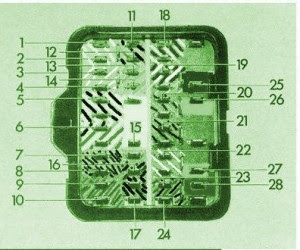
Fuse Panel Layout Diagram Parts: inside mirror electrochromic, interior light, light module, make up mirror light, navigation, on board computer, outside mirror, parking aid, passenger compartment, radio, rain sensor, rear wiper, roler sun blind, secondary air pump, side airbag, socket, speed control, starter interlock, telephone, trailer coupling, window lift, windscreen washer.

11W Stereo 22W Mono Power Amp Using TDA1519C

Posted by Unknown 0 comments
Integrated AF power amps have seen great improvements in recent years offering improved power and easier use. The TDA1519C from Philips contains two power amplifiers providing 11 W per channel stereo or 22 W mono when the two channels are connected in a bridge configuration. The special in-line SIL9P package outline allows the chip to be conveniently bolted to a suitable heatsink. The TDA1519CSP is the SMD version, in this case the heat sink is mounted over, and in contact with, the top surface of the chip.

11W Stereo Mono Power Amp Circuit Diagram Using TDA1519C
The operating voltage of this device is from +6V to +17.5V. The two channels of the amplifier are different in that one channel, between pins 1 and 4, is a non-inverting amplifier, while the other between pins 9 and 6 is an inverting amplifier. It is therefore necessary in stereo operation, to wire the speakers so that one of them has its polarity reversed. Each amplifier has an input impedance of 60kΩ and a voltage gain of 40dB, i.e. 100 times. When both amplifier are used in a bridge configuration, the inputs are in parallel so that the input impedance will be 30kΩ.

22W Mono Power Amp Circuit Diagram Using TDA1519C
A combined mute/standby function is provided on pin 8. In its simplest form this can be connected to the positive rail via a switch. When the switch is open the amplifier will be in standby mode and current consumption is less than 100µA. When the switch is closed, the amplifier will be operational. A circuit is also shown that uses the mute input to prevent the annoying switch-on plop heard when power amps are first switched on This is caused by the rush of current to charge capacitors C1 and C2.

standby switch circuit diagram
The circuit shown generates a ramp voltage, which is applied to pin 8. At switch on, as the voltage rises from 3.3 V to 6.4 V, the amplifier will switch out of standby mode and into mute mode allowing C1 and C2 to charge. Only when the ramp voltage on pin 8 reaches 8.5V will the amplifier switch into active mode. Protection built into the TDA1519C would seem to make it almost foolproof. The two outputs can be shorted to either of the supply rails and to each other. A thermal shutdown will prevent overloading and the power supply input is protected against accidental reversal of the supply leads up to 6V.

78xx Voltage Regulators

Posted by Unknown Monday, September 23, 2013 0 comments
The voltage regulators from the 78xx-series are found in many analogue power supplies. It seems, then, somewhat superfluous to say much more about them. But on the other hand, it can be very useful to highlight the important points, just because they are so ubiquitous. The 78xx is almost always used ‘bare’, because additional components are almost unnecessary. In fact, only one additional component is required, and that is capacitor C2. Based on the manufacturer’s recommendation, this capacitor should be 220nF in order to prevent oscillatory behavior. In practice, you will almost always see that a 100nF capacitor used here. This is a value that does not cause problems. C1 is the smoothing (reservoir) capacitor, its purpose is to reduce the ripple of the rectified AC voltage and is not actually related to voltage regulation.

If the DC voltage is provided by a mains adapter, then this electrolytic capacitor is usually already part of the adapter, although the value is rather small sometimes. C2 may only be omitted if C1 is close to the 78xx and C1 is of good quality (low ESR). But there is nothing wrong by playing it safe and always fitting C2. Rule of thumb: always place a 100 nF capacitor on the input as close to the regulator as is practicable. Strictly speaking, there is no need for a capacitor on the output. However, a capacitor of at least 100 nF (C3) ensures much-improved regulation with fast (several microseconds) changes in load current. In practice, a decoupling-capacitor is placed close to the power supply pins of many ICs. These can provide the same function, provided they are placed not too far away.
78xx Voltage Regulators Circuit DiagramAn electrolytic capacitor (C4) can be added for similar reasons: to catch slow (and fast, if it is a good capacitor) variations in load current. There is actually no compelling reason to deal with slow variations, because the IC is fast enough of regulating these on its own. Rule of thumb: always place an output capacitor of at least 100 nF preferably as close as possible to the IC with the greatest current consumption (read: greatest changes in current consumption). When building the circuit, it is important to connect the capacitors via the shortest possible path. So don’t use long wires or make large loops. Obtain the input voltage for the regulator directly from the connections of the smoothing capacitor, because the ripple is smallest there.

Finally, a few remarks about the temperature that a 78xx may run at. As a first approximation, if seem to burn your fingers when touching the regulator, the temperature of the regulator is above 60°C and a (small) heatsink is definitely recommended. It is not really a problem when the IC gets too hot, because it was designed in such a way that it will turn itself off when the temperature is too high. It doesn’t actually turn off, but the output current reduces when the temperature increases. When the internal temperature has reached 150°C, the output current will be only a little more than half the current delivered at 25°C. That is why it is possible that the output voltage of the regulator has dropped even though the output current is less than the rated current for the IC. A heatsink is the obvious solution. Rule of thumb: you should be able to touch the regulator (or the heatsink) without burning yourself. If not, then the heatsink has to be larger.

Preamplifier For Soundcard

Posted by Unknown 0 comments
This circuit can be used for inductive pick-up elements and dynamic microphones Most soundcards have a ‘line’ input and one for an electret (condenser) microphone. To be able to connect an inductive tape-recorder head or a dynamic microphone, an add-on preamplifier is needed. Even in this day and age of integrated microelectronics, a transistorised circuit built from discrete part has a right of existence. The preamplifier described in this short article goes to show that it will be some time before discrete transistors are part of the silicon heritage. The preamplifier is suitable for use with a soundcard or the microphone input of a modem. As you will probably know, most sound-cards have input sockets for signals at line level (stereo), as well as one for a (mono) electret microphone.

For the applications we have in mind, connecting-up an inductive pick-up element or a dynamic microphone, both inputs are in principle suitable, provided the source signal is amplified as required. The author eventually chose the microphone input on the soundcard. Firstly, because the line inputs are usually occupied, and secondly, because the bias voltage supplied by the micro-phone input eliminates a separate power supply for the preamplifier. The microphone input of a soundcard will typically consist of a 3.5-mm jack socket in stereo version, although only one channel is available. The free contact is used by the soundcard to supply a bias voltage to the mono electret microphone. This voltage is accepted with thanks by the present preamplifier, and conveniently obviates an external (mains adaptor) power supply.

Preamplifier For SoundcardA classic design:

In true transistor-design fashion, the preamplifier consists of three stages. Capacitor C1 decouples the signal received from the microphone or pick-up element, and feeds it to the input of the first stage, a transistor in emitter configuration, biased to provide a current amplification of about 300 times. Together with the source impedance of the microphone or pick-up element, capacitors C2 and C3 form a low-pass filter which lightly reduces the bandwidth. In addition, the output low-pass, R2-C3, reduces the dynamic collector resistance at higher frequencies. In this way, the filter reduces the gain in the higher part of the frequency spectrum and so helps to eliminate any oscillation tendencies.

The first, high-gain, stage is terminated by T2. Unlike T1, this transistor does not add to the overall gain, because the output signal is taken from the emitter (common-collector circuit). T2 thus acts as an impedance converter, with C4 reducing any tendency to oscillation. The output stage around T3 is a common-emitter circuit again. In it, preset P1 determines the voltage amplification. T3 is biased by means of a direct-current feedback circuit based on components R7 and C5. To this is added an ‘overruling’ dc feedback path back to the input transistor, via R6. This measure guarantees good dc stability in the preamplifier. The circuit is small enough to be built on a piece of veroboard or stripboard, and yet remain reasonably compact.

To prevent interference from external sources, the completed board should be mounted in a properly screened (metal) enclosure, with the connections to the input source and the sound card made in screened cable. The preamplifier provides a frequency-linear response. In case the source signal is marked by frequency correction (e.g., RIAA), then a matching linearization circuit should be used if the relevant signals are used by the computer.

Dual Power Supply For Amplifiers

Posted by Unknown Sunday, September 22, 2013 0 comments
A power supply suitable for use with the 60W amplifier presented in the predeeding project is perfectly simple, and no great skill is required to build (or design) one. There are a few things one should be careful with, such as the routing of high current leads, but these are easily accomplished. The first thing to choose is a suitable transformer. I suggest toroidal transformers rather than the traditional "EI" laminated types because they radiate less magnetic flux and are flatter, allowing them to be installed in slimmer cases.

They do have some problems, such as higher inrush current at switch on, which means that slow blow fuses must be used. For the 60W amplifier, a nominal (full load) supply of +/- 35V is required, so a 25-0-25 secondary is ideal - however, see Updates, below. The circuit for the supply is shown below, and uses separate rectifiers, capacitors and fuses for each channel. Only the transformer is shared, so channel interactions are minimised. A single ±35V supply (i.e. using only a single bridge and set of filter capacitors) will work just as well in the majority of cases.

Dual Power Supply circuit diagram For AmplifiersThe 5A slow-blow fuse shown is suitable for a 300VA transformer, if a 120VA transformer is used, this should be reduced to 2.5A (or 3A if 2.5A proves too hard to get). If you are even a little bit concerned about the fuse rating, contact the transformer manufacturer for the recommended value for the transformer you will use. The correct fuse is critical to ensure safety from electrical failure, which could result in the equipment becoming unsafe or causing a fire.

The capacitance used is not critical, but is somewhat dependent upon ones budget. I suggest 10,000uF capacitors, but they are rather expensive so at a pinch 4,700uF caps should be fine - especially in the arrangement shown. When unloaded (or with only light load), the voltage will normally be somewhat higher than 35 Volts. This is Ok, and should not cause distress to any amp. The voltage will fall as more current is drawn, and may drop below 35V if a small transformer (or one with unusually poor regulation) is used.

Two parts of this circuit are critical:
  • Mains wiring must be cabled using approved 240V rated insulated cable, and all terminations must be insulated to prevent accidental contact. The mains earth must be securely fastened to the chassis, after scraping away any paint or other coating which might prevent reliable contact.
  • The centre-tap of the transformer and the ground points of each capacitor must be connected to the main signal earth point via heavy duty copper wire, or (preferably) a copper bus-bar. Large currents flow in this part of the circuit, containing nasty current waveforms which are quite happy to invade your amplifier. The supply voltages must be taken from the capacitors (not the bridge rectifiers) to prevent unwanted hum and noise.
When wiring the bridge rectifiers to the transformer, connect exactly as shown to ensure that ripple voltages (and currents) are in phase for each amp. If not, mysterious hum signals may be injected into the amps signal path from bypass capacitors and the like. This is somewhat unlikely unless huge caps are used on the amp board(s) - not recommended, by the way - but why take the risk?

Bridge rectifiers should be the big bolt-down 35A types (or something similar) to ensure lowest possible losses (these will not require an additional heatsink - the chassis will normally be quite sufficient). The transformer primary voltage will obviously be determined by the supply voltage in your area (i.e. 120, 220 or 240) and be suited to the local supply frequency. Note that all 50Hz transformers will work just fine at 60Hz, but some 60Hz devices will overheat if used at 50Hz.

The transformer should be rated at a minimum of 120VA (Volt-Amps) for home use, but a 300VA transformer is recommended due to its superior regulation. Going beyond 300VA will serve no useful purpose, other than to dim the lights as it is turned on. Where it is possible, the signal and power ground should be the same (this prevents the possibility of an electric shock hazard should the transformer develop a short circuit between primary and secondary. Where this will give rise to ground loops and hum in other equipment, use the method shown.

The resistor R1 (a 5W wirewound resistor is suggested) isolates the low-voltage high-current ground loop circuit, and the diodes D1 & D2 provide a protective circuit in the event of a major problem. These diodes need only be low voltage, but a current rating of 5A or greater is required. The 100nF capacitor (C1) acts as a short circuit to radio frequency signals, effectively grounding them. This should be a device with very good high frequency response, and a monolithic ceramic is recommended.

Updates:

The transformer secondary voltage will probably need to be higher than described above. I tested some stock and custom transformers I have, and found that unless the transformer has extraordinarly good regulation, a nominal 28-0-28 secondary will be needed, more with an average (i.e. poor) regulation unit. Also be careful when you test, since a relatively small (10%) variation in the mains voltage makes a big difference to measured output power - the secondary voltage also falls by 10%, so 60W becomes 48W if the mains is 10% low.

You also need to remember that the output voltage of transformers is typically quoted at full power with a resistive load. This means two things:
  1. The no load voltage will be higher than expected
  2. The loaded voltage will be lower than expected
The first point is true because there is no loading, so the output voltage must rise. The second is more complex, but happens because the conventional rectifier circuit uses a capacitor input filter (the rectifier feeds directly into the capacitor(s)). Since the diodes only conduct at the peak of the waveform, the current is much higher, so the transformer and supply line impedance will cause the peak voltage to fall, and the DC voltage cannot exceed the peak output voltage (less two diode forward voltage drops).
Source: http://sound.westhost.com/project04.htm

Mains Indicator

Posted by Unknown 0 comments
It is not always immediately obvious whether a power-consuming appliance is switched on or not. Examples are the lamp in the attic or the shed, or electric heating in an awkward place. A nice solution would be to connect an LED directly in series with the appliance, unfortunately you’d better duck for cover if you tried… The obvious solution would be to place a (power-) resistor in series with the load and connect an LED with series resistor across it.

However, this solution has significant disadvantages, for instance, the power loss is relatively large (easily a few watts). In addition, the value of the resistor should be adjusted depending on the magnitude of the current. It would be better to insert two anti-parallel diodes in the power lead. Unfortunately, the voltage drop is too low to power an LED. It does work with 6 diodes, for that matter, but the power loss is then also 3 times greater.

Mains Indicator circuit schematic

We therefore chose a solution with two diodes, followed by a 4 times voltage multiplier in the form of a cascade rectifier. That is an energy friendly solution. The current through the LED is automatically limited by the internal impedance of the cascade rectifier. The impedance isn’t that small, despite the large electrolytic capacitors. Use a low-current LED, otherwise the LED will probably not be bright enough.

Parts layout:
Parts Layout Of Mains Indicator circuit schematic

The 1N5404 used here can handle up to 3 A (3 A × 230 V = 690 W). If the power is less than 200 W, you could use two 1N4004s instead. The voltage across the diodes is a square wave with an amplitude of about 1.3 Vpp. The voltage multipliers are used to turn this into the LED voltage. This will only work if the voltage drop across the diodes in the multipliers isn’t too large. That is why these diodes are Schottky diodes. These only have about a 0.35 V voltage drop.

PCB layout:
PCB Layout Of Mains Indicator circuit schematic

Exactly which type of Schottky diode that you use is not too important. You are free to experiment with the value of the electrolytic capacitors. The larger their value, the greater is the amount of current that can be delivered. Keep in mind that working with mains voltage can be fatal. Build the circuit in such away that there is no risk that live parts can be touched and maintain isolation distances of 6 mm (also in air). For the same reason, use a 5 mm LED (not a 3 mm one!) and fit it as far into the enclosure as possible. Mount the PCB in the enclosure with nylon bolts.

COMPONENTS LIST
Capacitors:
C1-C4 = 220µF 6.3V
Semiconductors:
D1,D2 = 1N5401
D3-D6 = BAT85 (or any other Schottky diode)
D7 = LED, low current
Miscellaneous:
K1 = 2-way PCB terminal block, lead pitch 5mm

1966 ford thunderbird Wiring Diagram

Posted by Unknown Saturday, September 21, 2013 0 comments
1966 ford thunderbird Wiring Diagram
(click for full size image)

The Part of 1966 ford thunderbird Wiring Diagram: fuse block, stop light switch, backup light switch, neutral safety switch, blower motor, temp gauge, oil switch, breaker, alternator.

Fuse Box BMW Z4 2005 Coupe Diagram

Posted by Unknown 0 comments
Fuse Box BMW Z4 2005 Coupe Diagram - Here are new post for Fuse Box BMW Z4 2005 Coupe Diagram.

Fuse Box BMW Z4 2005 Coupe Diagram


Fuse Box BMW Z4 2005 Coupe Diagram

Fuse Panel Layout Diagram Parts:air bag, ASC/DSC, CD charger, central locking system, low beam headlight, lighting circuit, high beam headlight, brake light, interior and luggage, cigar lighter, side light, turn indicator.

Fuse Box BMW 02 Touring 1971 Diagram

Posted by Unknown Friday, September 20, 2013 0 comments
Fuse Box BMW 02 Touring 1971 Diagram - Here are new post for Fuse Box BMW 02 Touring 1971 Diagram.

Fuse Box BMW 02 Touring 1971 Diagram


Fuse Box BMW 02 Touring 1971 Diagram

Fuse Panel Layout Diagram Parts: parking, side light, license plate light, instrument lighting, fog warning light, fog lamp relay, low beam headlight, indicator flasher, cigar lighter, clock, insterior light, hazard warning flasher, trailing turn indicator, heater blower, fuel pump, automatic choke, fuel gauge, coolant thermometer, oil pressure telltale, stop light, run indicator light, washer, wiper motor, reversing light.

1996 Chevrolet Camaro Z28 Wiring Diagram

Posted by Unknown Thursday, September 19, 2013 0 comments
1996 Chevrolet Camaro Z28 Wiring Diagram

The Part of 1996 Chevrolet Camaro Z28 Wiring Diagram: instrument cluster, tachometer, black wire, yellow wire, red wire, crankshaft, power distribution,camshaft position sensor, tachometer output, sensor ground, sensor ignition positive voltage, tachometer output, reference sigal, knock sensor, srankshaft position sensor, underhood electrical center, sensor ignition positive voltage, bypass control, powertrain control module.

Smart Lighting in the Enterprise

Posted by Unknown Thursday, September 12, 2013 0 comments
Daylight harvesting is becoming increasingly important in the design and implementation of commercial lighting systems. Being able to integrate the natural light from windows with flexible, controllable sources of lighting helps improve the work environment and cut energy bills.
Smart Lighting in the Enterprise
Being able to have closer control of the lighting systems in a commercial environment is a key element to this strategy and energy harvesting can play an important role. Being able to have flexible placement of control pads for a commercial lighting system is an important requirement as office space is regularly reconfigured as existing clients grow and change their requirements and new clients have new requirements.

Build a Cell Phone Jammer Schematic Diagram

Posted by Unknown Wednesday, September 11, 2013 0 comments
Build a Cell Phone Jammer Schematic Diagram
 
This cell phone jammer operates at GSM800 frequency since most mobile phones use it to operate. So the selected VCO is a sweeping oscillator, which is very effective but may be hard to construct for the beginners without nice RF-testing equipment.

As a noise source you can use 45MHz clock oscillator which is driving Local Oscillator port located on a mini-circuit mixer. There is also an impedance matching network for Local Oscillator signal to pass through it. It is used to equate impedances of the clock oscillator and the port of the mixer.

RF input (which is this port of the mixer) connected to the first 800MHz cell phone antenna, and the RF output is sent to the mini-circuit amplifier. This amplifier increases the output power for 15-16dbm. The amplified signal then sent to the second cell phone antenna.

Build a Cell Phone Jammer Schematic Diagram


 works
All cell phones which use GSM800 have their transmitted and received frequencies always separated by 45MHz. So when the mobile phone tries to call it is blocked by its own signal returning to it! Isn’t that cool? When the phone blabber annoys you – turn your jammer on and that wrongdoer will hear own voice in his or her cell phone.

Oh, by the way, you can also use this mobile signal jammer to block any cell-based tracking systems which use your GPS to track and record your car’s moves. And it is quite possible (though I didn’t actually tested it) to jam IEDs which detonated using cell phones.

Build a Cell Phone Jammer Schematic Diagram


The mixer used is designed to work up to 600MHz but in this case it works pretty well.

Build a Cell Phone Jammer Schematic Diagram
 
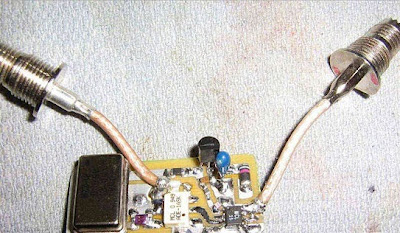
RF amplifier is doing its job perfectly yet (as it was mentioned in the Jammer Store blog post) draws additional power.Old aluminium box was used as a frame for the jammer and old UHF connectors from Motorola cell phone as input/output.You need to attach RF connectors to the circuit. Nine volt battery and voltage regulator were used to supply all components. The battery was placed inside and separated by the foamed plastic from the other components.The power on/off switch is placed on the top. The input and output antennas (also from old Motorola mobile phone) are screwed onto UHF connectors.Your cell phone jammer is ready. Enjoy!

Build a Cell Phone Jammer Schematic Diagram


Over voltage Protection Circuit Diagram

Posted by Unknown 0 comments
When testing a circuit, a source of voltage that is variable and has over voltage shutdown is veiy useful. In this circuit, Rl is adjusted to 1 to 2 V below the eventual shutdown threshold. R2 sets the trip voltage. When this voltage is reached, the circuit shuts the voltage to the circuit under test down. To reset, reduce Rl below trip threshold and depress reset switch SI.

Over voltage Protection Circuit Diagram

Overvoltage Protection Circuit Diagram

Compressor Bleed Air Valve Actuation

Posted by Unknown Tuesday, September 10, 2013 0 comments
Compressor Bleed Air Valve Actuation

1 W Home Stereo Amplifier Circuits Diagram

Posted by Unknown 0 comments
This is a one watt home stereo amplifier module project using the KA2209 IC from Samsung, which is equivalent to the TDA2822. It operates from 3-12V DC & will work from a battery since the dormant current drain is low. It requires no heat sink for normal use. The input & output are both ground referenced. Maximum output will be obtained with a 12V power supply & 8 ohm speaker, however it is suitable for driving headphones from a supply as low as 3V.

The Specifications of the home stereo amplifier :

D.C. input : 3 – 12 V at 200 – 500 mA max
Idle current : approx. 10 mA
Power output : > 1 Watt max. 4-8 ohms, 12V DC
Freq. Resp. : approx. 40 Hz to 200 kHz, 8 ohm, G=10
THD : < 1 % @ 750 mW, 4-8 ohm, 12V
Gain : approx. x10 (20 dB) OR x100 (40dB)
S/N ratio : > 80 dB, G = 20 dB
Sensitivity : < 300 mV, G = 20 dB
Input Impedance : approx. 10 k ohm

Description 

The gain is adjustable from ten to 100, i.e. twenty to 40 dB. Start with feedback resistors R1 and R3 of 1k ohm, this will give a gain of ten which ought to be adequate for most applications. In case you need more gain, you can remove resistors R1 and R3.This will give a gain of about 100, or 40 dB.The input attenuation can be adjusted by the potentiometer which can be used as a volume control. The IC gain ought to be kept as low as necessary to accomplish full output, with the in put potentiometer and your signal source at maximum.

1 W Home Stereo Amplifier Circuit Diagram

1 W Home Stereo Amplifier


Voltage Gain = 1+ R1/R2 = 1+R3/R4, however the maximum gain with no outside feedback is about 100, or 40dB. (GdB = 20log Gv)

This will keep the signal to noise ratio as high as feasible. Additional gain provided by the amplifier will reduce the S/N ratio by a similar amount, since the input noise figure is constant. Other values for R1 and R3 of between 1k and 10k ohm can be used if an intermediate gain level is necessary.

If driving a pair of headphones, you may also need a 100 ohm resistor in series with each output to reduce the output level, depending on headphone impedance & sensitivity. Make positive you start with the volume right down to check. Numerous headphones may be driven from the amplifier in the event you wish, since most headphones have at least 16 ohm impedance, or more often 32 ohm.

There are only a few outside parts, the IC contains most of the necessary circuitry. R1,R2 and R3,R4 are the feedback resistors. C1 provides power supply decoupling. C2 and C3 are the input coupling capacitors, which block any DC that might-be present on the inputs. C4,C5 block DC in the feed back circuit from the inverting inputs, and C6,C7 are the output coupling capacitors. C8, R5 and C9,R6 act as Nobel networks providing a high frequency load to maintain stability at frequencies where loud speaker inductive reactant may become excessive. The pot provides adjustable input level attenuation.

1 W Home Stereo Amplifier parts list

Arduino Leonardo vs Uno

Posted by Unknown Monday, September 9, 2013 0 comments
The Arduino team is now shipping their latest creation – the Leonardo. It is the first Arduino to use Atmelʼs ATmegaXU4 series chip with built-in USB. This change is big and it has big benefits. In addition to the built-in USB, it offers more digital and analog pins. This comprehensive guide gives you the details you need to know to start using it – pinout differences, hardware capabilities, new software libraries and more.
Arduino Leonardo vs Uno – What’s New

13 Color LED Rainbow Schematic

Posted by Unknown Thursday, September 5, 2013 0 comments
Only a few years ago, the choice of LEDs was limited to IR, red, yellow, and green. The LED manufacturers have been busy extending the spectrum, and filling in the gaps. The latest generation of organic LEDs (OLEDs) has added some dazzling new colors to the spectrum. This circuit uses a set of 13 differently colored LEDs to generate a full color spectrum. The photo does not fully represent the colors generated due to camera limitations. The real-world display is very eye-catching. If you want to "trick out" your PC, this circuit is for you. Forget about those boring blue PC light displays.

13 Color LED Rainbow Circuit Diagram:


13 Color LED Rainbow

Specifications:
  • Operating Voltage: 6-12V DC
  • Operating Current: 145ma at 12V DC
Theory:
The LM2940T-5.0 low dropout voltage regulator converts the 6-12V DC input power to regulated 5 Volts. It was chosen over a standard 7805 regulator so that the circuit could maintain regulation while operating on a 6V battery. The 1N4001 diode protects the circuit from reverse polarity, if a battery or power supply capable of generating over 1 amp is used, a 1 amp fuse should be installed between the supply and the circuit. The 5 Volts is used to drive each of the LEDs through individual current limiting resistors.

The resistor values were determined experimentally for equal brightness. Values are given as examples only, different sources of LEDs will require different resistor values. Resistor selection turns out to be the most difficult part of the circuits construction. A 100 ohm resistor in series with a 1K pot could be used in place of each resistor if individual brightness adjustments are desired. The table below lists the LED colors and wavelengths.

LED Color Wavelength Description
Deep Red 700nm ---------
Red 660nm traditional red
Orange Red 635nm "high efficiency" red
Orange 623nm also called red orange
Amber 594nm ---------
Yellow 588nm & traditional yellow
Yellow Green 567nm traditional green
True Green 523mn --------
Cyan 501nm verde green, blue green
Aqua 495?nm ---------
Deep Blue 470nm ultra blue
Powder Blue 430nm first generation "powder blue"
Violet 410nm ---------

Construction:
The circuit was built on a prototype perforated board with printed solder pads. The circuitry is hand-wired on the back side of the board. Care should be taken when soldering to the LEDs, a clip-on heat sink should be used while soldering the leads. Care should be taken to avoid zapping the LEDs on the violet side of the spectrum, they are sensitive to static electricity. The circuit board can be mounted on a piece of white hardboard, the white paint reflects the colors nicely.

Use:
Apply power to the circuit and enjoy the colorful glow. Do not stare directly into the array at close range for extended periods, some of the LEDs are extremely bright.

Taking The Circuit Further:
The spectrum could be extended on both the IR and UV sides. A brief scan through the Mouser catalog indicates the availability of these IR wavelengths: 940nm 880nm, 875nm, 870nm, 850nm. UV LEDs at 400nm, 395nm and 380nm are also available. There are also many LED colors available with wavelengths between the 13 colors shown, the colors selected were chosen for an evenly spaced color spectrum.

13 Color LED Rainbow

An open-collector LED driver circuit could be connected to the negative LED leads for computer control.The circuit could be used in conjunction with a photo detector for characterizing optical filter curves. Typically, the photo detector output is sent to a logarithmic converter, the log-ratio of the direct light versus the filtered light characterizes the attenuation at a given wavelength.

Parts:
Most of the LEDs were purchased from Digi-Key, Jameco, and Mouser. All of the parts were T1-3/4 size, clear packages were used wherever possible. LEDs from different manufacturers may have different focus characteristics. All of the resistors are 1/4 Watt parts. LED part numbers are not available, the rainbow was assembled from parts that were accumulated over several years. Beware that different LED manufacturers use different names for their colors, the wavelength is the best indicator of the color. The Aqua LED is the most difficult part to find, All Electronics carries them, although the wavelength is unspecified.
 

Car Battery Charger Circuit

Posted by Unknown Wednesday, September 4, 2013 0 comments
Description
This charger will quickly and easily charge most any lead acid battery. The charger delivers full current until the current drawn by the battery falls to 150 mA. At this time, a lower voltage is applied to finish off and keep from over charging. When the battery is fully charged, the circuit switches off and lights a LED, telling you that the cycle has finished.
Circuit Diagram
Parts
R1 500 Ohm 1/4 W Resistor
R2 3K 1/4 W Resistor
R3 1K 1/4 W Resistor
R4 15 Ohm 1/4 W Resistor
R5 230 Ohm 1/4 W Resistor
R6 15K 1/4 W Resistor
R7 0.2 Ohm 10 W Resistor
C1 0.1uF 25V Ceramic Capacitor
C2 1uF 25V Electrolytic Capacitor
C31000pF 25V Ceramic Capacitor
D1 1N457 Diode
Q1 2N2905 PNP Transistor
U1 LM350 Regulator
U2 LM301A Op Amp
S1Normally Open Push Button Switch
MISC Wire, Board, Heatsink For U1, Case, Binding Posts or Alligator Clips For Output
Notes
1. The circuit was meant to be powered by a power supply, which is why there is no transformer, rectifier, or filter capacitors on the schematic. There is no reason why you cannot add these.
2. A heatsink will be needed for U1.
3. To use the circuit, hook it up to a power supply/plug it in. Then, connect the battery to be charged to the output terminals. All you have to do now is push S1 (the "Start" switch), and wait for the circuit to finish.
4. If you want to use the charger without having to provide an external power supply, use the following circuit.
 Circuit Diagram

C1 6800uF 25V Electrolytic Capcitor
T1 3A 15V Transformer
BR1 5A 50V Bridge Rectifier 10A 50V Bridge Rectifier
S1 5A SPST Switch
F1 4A 250V Fuse
5. The first time you use the circuit, you should check up on it every once and a while to make sure that it is working properly and the battery is not being over charged.
Author:
Source: http://www.aaroncake.net

MC2833 FM Transmitter

Posted by Unknown 0 comments
A very simple FM transmitter circuit can be designed using MC2833 integrated circuit, designed for cordless telephone and FM communication equipment. It includes a microphone amplifier, voltage controlled oscillator and two auxiliary transistors.This MC2833 FM transmitter circuit has an low drain current ( ICC =2.9mA typically ) and supports a wide range operating voltage ,from 2.8 to 9 volts .

MC2833 FM Transmitter
Crystal X1 connected at pin 16 and pin 1 ( trough a 5.1uH coil ) is fundamental mode, calibrated for parallel resonance with a 32 pF load.The final output frequency is generated by frequency multiplication within the MC2833 IC. The RF output buffer (Pin 14) and Q2 transistor are used as a frequency tripler and doubler, respectively, in the 76 and 144 MHz transmitters.


The Q1 output transistor is a linear amplifier in the 49.7 MHz and 76 MHz transmitters, and a frequency doubler in the 144 MHz transmitter.All coils used are 7 mm shielded inductors, CoilCraft series M1175A, M1282A–M1289A, M1312A or equivalent.Power output is 9 + 10 dBm for 50 MHz and 76 MHz transmitters, and 9 + 5.0 dBm for the 144 MHz transmitter at VCC = 8.0 V. Power output drops with lower VCC.

PIC Digital Clock Timer

Posted by Unknown Tuesday, September 3, 2013 0 comments
his clock timer uses a PIC16F628 microcontroller to display 3 and 1/2 digit time and control an external load. The clock includes a calendar with leap year and optional daylight savings adjustments. The timer output can be set from 1 to 59 minutes and manually switched on and off. The clock also has a correction feature that allows an additional second to be added every so many hours to compensate for a slightly slow running oscillator.  The oscillator uses a common 32.768 KHz watch crystal and the frequency can be adjusted slightly with the 24pF capacitor on the right side of the crystal.

There are 7 displays that advance each time the D switch is toggled. To make adjustments, set the RA5 switch to the "B" position and then toggle the E and F switches to advance the data in the hours or minutes digits. Then toggle the "D" switch to move to the next data. After the 7th display, it will go back to the top and display the current time. Or, just press the time switch C to get to the top at anytime. When done setting everything up, set the RA5 switch to the "A" position so the data cannot be accendentally changed. You can still view everything with the "D" advance key, but the E an F switches will just turn on or off the alarm at RB7. I use it with an external transistor to switch on and off a radio.

PIC Digital Clock Timer Circuit Diagram


The Daylight savings setting (in the 6th display in the minutes digits) is used to enable daylight savings time adjustments, one hour ahead on the 2nd sunday in March, and one hour behind on the first sunday in November. The entry will be either 0, 1, or 3.

0 = Daylight savings time disabled (default).
1 = Savings time enabled and current time is standard time.
3 = Savings time enabled and current time is daylight savings time.

The last 2 entries on the list (Year and Correction) is for the current year (1 to 4) (4 = Leapyear) so todays setting (2006) will be 2 since leapyear will be on year 4 which is 2 years from now. The correction setting will add a second every so many hours for fine adjustment to the oscillator frequency. My setting is 18 which adds a second every 18 hours. Its pretty accurate and only loses 3 seconds a month. You probably want to run it for a couple weeks to figure out what correction is needed for the crystal you have.

Switch functions:

RA0         (C switch)         =  Display Time
RA1         (D switch)         =  Advance to next data (alarm, calendar, etc)
RA2, RA3    (E and F switch)   =  Advance hours and minutes (in setup mode).
RA2, RA3    (E and F switch)   =  Toggle alarm output on/off (in run mode)
RA5 in the B position (open) =  Setup Mode

Download asm file

100 W Bipolar Power Amplifier

Posted by Unknown 0 comments
This is a basic 100 watt power amplifier designed to be (relatively) easy to build at a reasonable price. It has a better performance (read: musical quality) than the standard STK module amps that are used in almost every mass market stereo receiver manufactured today.

100 W Bipolar Power Amplifier Circuit Diagram


When I originally built this thing, it was because I needed a 100 WPC amp and do not want any money. So I designed around parts I had in the store. The design is actually a standard format, and I’m sure there are commercial entities that are similar. To my knowlwdge, it is not an exact copy of a commercial entity, nor am I aware of any patents on topology.

For experienced builders: I am aware that many improvements and adjustments can be made, but the idea was to keep it simple and must do-able by anyone who is a circuit, and has not the patience to do a sloppy job. If friend want Bipolar Transistor power amplifier circuit. , In model HIFI OCL 100W RMS. I think this track should be an interesting choice, this circuit is the use of the key transistor BD317 and BD318 unless transistor number BD139, BD140, BC556 too easy then try to buy when the 35V power source with only then build is not difficult for other details as the result of a few See Circuit.

Input stage is a BC556 transistor, which most of the open loop gain, and on the serene DC voltage stabilizes. This feeds a level shift stage where the voltage swing to (-) track references. The Transconductance stage is a Darlington, improve frerqency high linearity. The BD317, 318 on a rather large collector-base capacity is dependent on voltage. The BD319 presents this low-z and has a C (ob) of only a few of PF, which is effectively swamped by the pole-splitting 220pF cap. The scene is supplied by BC546 active load (current), which is approximately 20 mA. The current, until the BC556 is limited to about 70 mA in the worst cases.

Lithium Polymer Peak Charger Circuit Diagram

Posted by Unknown Monday, September 2, 2013 0 comments
Description
This circuit was developed to charge the Lithium-Polymer cells used in a model aircraft. Lithium-Polymer cells are incredibly lightweight compared to Ni-cad battery packs of the same voltage and amp-hour rating. Their only drawback is that they require a rigid charge and discharge regime to achieve maximum life. The most important points of note are as follows:
Circuit Diagram:

  1. They should be charged using a constant-current, constant-voltage method, which stops the charge once the current has dropped to about the C/10 rate. For example, for an 800mAh pack, charging should be terminated once the current falls to approximately 80mA.
  2. They should never be discharged below 3V per cell otherwise they will be permanently damaged.
  3. should not be charged or discharged above their rated current otherwise an explosion and fire can result!
To initiate charging, the momentary "Start" button (switch S1) is pressed, closing the relay contacts and connecting the battery pack to the output of REG1. The circuit will then charge two 800mAh cells in series at a constant current of 600mAh until they reach a peak terminal voltage of 4.2V per cell (nominal terminal voltage for these cells is 3.7V).
REG1 and transistor Q2 form a current-limited voltage regulator. When the charge current exceeds about 600mA, the voltage developed across R7 turns on Q2, which in turn pulls the adjust terminal of REG1 towards ground. This shunts the voltage adjustment resistance chain formed by VR2 and R3, thereby limiting the output to 600mA.
When the battery voltage reaches about 8.4V, the regulator limits any further voltage increase, as set by VR2. The charge current will then slowly decrease as the cells reach full capacity. As a result, the voltage across R7 also falls, until the bias voltage on the base of Q1 is too small to keep it in conduction. When Q1 turns off, the relay also turns off, isolating the fully charged battery.
The charger is set up as follows:
  1. It to 12V DC and place a digital voltmeter between the output of REG1 and the negative output for the battery pack. Adjust VR2 for a reading of 8.4V.
  2. VR1 so that the voltage on the base of Q1 is at maximum.
  3. Place an ammeter in series with the battery to be charged and press the "Start" button. The output current will shoot up to around 600mA, then slowly decrease over the next one to two hours.
Once it falls to around 80mA (or whatever the C/10 rate is for your cells), slowly turn VR1 until the relay switches off and indicator LED goes out.
The circuit should now charge your battery packs to within 97% of their rated capacity.
Finally, note that in most cases, REG1 will need to be fitted with a heatsink.
 Source - Silicon Chip January 2005